Download

1 / 10
110 likes | 286 Views
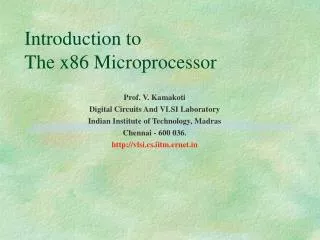
EE466/586 VLSI Design. Partha Pande School of EECS Washington State University pande@eecs.wsu.edu. Lecture 26 Memory Design (Cont’d). BL. 1. BL. 2. WWL. RWL. M. 3. X. M. 1. M. 2. C. S. No constraints on device ratios. Reads are non-destructive.

E N D
EE466/586VLSI Design Partha Pande School of EECS Washington State University pande@eecs.wsu.edu
Lecture 26 Memory Design (Cont’d)
BL 1 BL 2 WWL RWL M 3 X M 1 M 2 C S No constraints on device ratios Reads are non-destructive Value stored at node X when writing a “1” = V -V WWL Tn 3-Transistor DRAM Cell
3-Transistor DRAM Cell • Precharge both the columns • Assert the write word line (WWL) • The data is retained as charge on capacitance CS once WWL is lowered • When reading the cell, the read-word line (RWL) is raised • If “1” is stored then BL2 will be discharged through M3 and M2 • If “0” is stored then there will be no conducting path,, so the precharged high level of BL2 will not change significantly.
C S ------------ V V D = – V = V – V BL PRE BIT PRE C + C S BL 1-Transistor DRAM Cell Write: C is charged or discharged by asserting WL and BL. S Read: Charge redistribution takes places between bit line and storage capacitance Voltage swing is small; typically around 250 mV.
DRAM Cell Observations • 1T DRAM requires a sense amplifier for each bit line, due to charge redistribution read-out. • DRAM memory cells are single ended in contrast to SRAM cells. • The read-out of the 1T DRAM cell is destructive; read and refresh operations are necessary for correct operation. • Unlike 3T cell, 1T cell requires presence of an extra capacitance that must be explicitly included in the design. • When writing a “1” into a DRAM cell, a threshold voltage is lost. This charge loss can be circumvented by bootstrapping the word lines to a higher value thanVDD
Content-Addressable Memories (CAMs) • In SRAMs the access mechanism is based on known address. • But there are applications where the data we seek is associated with a known binary keyword rather than a known binary address. • The known keyword is compared against previously stored keywords, called tags, that reference the actual data we seek • The tags are not stored in any particular order so we must match the address keyword with the tags that are already stored to access the desired data.
Static CAM Memory Cell Bit Bit Bit Bit Bit Bit Word M8 M9 M4 M5 CAM ••• CAM M6 M7 ••• ••• Word S S Word int CAM ••• CAM M3 M2 Match M1 Wired-NOR Match Line
Principle • The array contains n-bit stored tags that are to be compared with the incoming n-bit keyword. • Each row holds a different tag • Each bit of the tag is stored in a separate 6T SRAM cell. • Match lines are pre charged high • If there is a match, the match line remains high • If the keyword and stored tag do not match, the NMOS device discharges the match line.
CAM in Cache Memory CAM SRAM ARRAY ARRAY Hit Logic Address Decoder Input Drivers Sense Amps / Input Drivers Address Tag Hit R/W Data