Download
1 / 22
220 likes | 321 Views
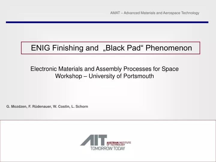
ENIG Finishing and „Black Pad“ Phenomenon. Electronic Materials and Assembly Processes for Space Workshop – University of Portsmouth. G. Mozdzen, F. Rüdenauer, W. Costin, L. Schorn. Content. Metallographic investigations of PCBs with ENIG finishing with respect to “Black Pad” phenomenon.

E N D
ENIG Finishing and „Black Pad“ Phenomenon Electronic Materials and Assembly Processes for Space Workshop – University of Portsmouth G. Mozdzen, F. Rüdenauer, W. Costin, L. Schorn
Content Metallographic investigations of PCBs with ENIG finishing with respect to “Black Pad” phenomenon PCB – short time in use – detachment of BGA – failure analysis -Investigation of BGA and corresponding area on PCB -Investigation of conductive paths PCB after 100 thermal cycles in the temperature range between -10 and +60°C PC boards have been delivered by ESA-ESTEC
Methods Light Microscopy (inverse metallographic microscope) High Resolution Scanning Electron Microscopy (HRSEM) Energy Dispersive Spectroscopy (EDS) Focused Ion Beam (FIB – CrossBeam Workstation)
PCB BGA What is “Black Pad”? Failure AnalysisAssumption “Black Pad” BGA - Bonding traces on solder balls PCB - Bonding traces on conductive pads
“Black Pad” – Definition “Black Pad” phenomenon – black or grey appearance of the conductive pads. It causes poor solderability and consequently it is responsible for weakness of solder joints. Origin of “Black Pad” - corrosion of Ni during the Nickel deposition (e.g. M. Walsh) or/and during the Gold Immersion process (e.g. R. A Bulwith, N. Biunno,..,) and formation of P-rich layer on the top of EN film. The corrosion process starts on the Nickel nodule boundaries causing spikes and propagates inside the nodules . On the corroded surface no or very poor IMCs developed during soldering. The corrosion due to IG process can be control by sufficient IG-bath parameters (e.g. pH, temperature, process duration). III: Solder joint - IMCs embedded in P-rich “underground” as a result of II or I+II II: Soldering - P- enrichment on the interface; EN-to-solder due to formation of IMCs I: ENIG finishing – P enrichment on EN surface due to corrosion (Ni-bath, Au-bath) No “Black Pad” phenomenon “Black Pad” phenomenon Solder Joint and P - enrichment
PCB 20 kV – high activation volume information from large volume BGA To early for conclusions an indication of “Black Pad” but no an evidence 10 kV – low activation volume information from area close to the surface BGA detached from PCB / EDS Surface Analysis Q; How can we prove a P enrichment on the detached surfaces? A; By using low and high accelerating voltages Conclusion Failure (detachment) due to “Black Pad” effect
EDS Surface Analysis – Interface Composition It has been reported that during reflow Ni3P has formed, consequently the black interlayer between IMCs and EN-film consists predominately of this phase (P. Snugovsky – Celestica Inc., Materials Science Lab.), Q; Could we confirm such a finding taking into account our results of chemical analysis? Q; Did Sn enrich on the pads surface ? A; we can not confirm observation of P. Snugovsky The top of EN film consists of P , only small amount of Ni3P possible A; According to EDS surface analysis - yes
BGA detached from PCB / Surface Analysis BGA PCB Elongated convex structures on the BGA side correlate with elongated concave structures on the PCB side High density of elongated convex structures (width < 1µm) High density of elongated concave structures (width < 1µm)
BGA detached from PCB / Surface Analysis Q; What is the chemical composition of the elongated structures? BGA PCB A; BGA side – the elongated convex structures consist predominately of Pb. A; PCB side – the elongated concave structures are partly filled with Sn.
BGA – Solder Ball - Cross Section Q; Do we observe IMCs ? BGA Solder Ball A; IMCs are present on the BGA surface, the width of IMC zone ~ 4 µm
BGA – Solder Ball - Cross Section Q; Which phases have formed during soldering? ~ NiSn (Ni3Sn4) ~ Ni3Sn7 A; NiSn and Ni3Sn7 could be detected by EDS analysis Brittle phase of the type Me3Sn ((Ni+Au)3Sn) which is believed to be detrimental for the strength of the bonding has not been identified
Sn Ni Cu P Au Pb PCB - Cross Sections The surface analysis revealed Sn inside the cavities as well as P and Sn enrichment on the surface (close to the surface) Q; Does analysis of the cross section confirm the results of the surface analysis ? FIB cut A; Results of the surface analysis have been confirmed by the results of the cross section analysis P-enrichment close to the surface, Presence of Sn on the surface The elongated concave structures are partly filled with Sn.
BGA detached from PCB / Summary BGA side PCB side Presence of IMC – ~NiSn, ~Ni3Sn7 No presence of the brittle phase - Ni3Sn High density of the elongated convex structures (width < 500nm) Elongated convex structures are predominately composed of Pb P-enrichment close to the EN surface (~300nm layer) P rich layer may contain small amount of Ni3P Presence of Sn on the surface (~ 100nm film) Presence of elongated concave structures Elongated concave structures are partly filled with Sn Elongated convex structures on the BGA side correlate with elongated concave structures on the PCB side
Additional Information needed for Interpretation and Conclusions Investigation of conductive paths present on PCB Area with middle stage of corrosion, distinct nodule boundaries
FIB cut Additional Information needed for Interpretation and Conclusions Investigation of conductive paths present on PCB Corroded nodule boundaries correlate with spikes - corrosion continuous from surface towards interior Black bands (Black Pad phenomenon) below Au film visible
Au film ~ 300nm Investigation of conductive paths present on PCB Conductive paths on the investigated PCB exhibit mostly an early stage of “Black Pad” phenomenon Black bands (“Black Pad” phenomenon) below Au film <~ 100nm P-enrichment - “Black Pad” phenomenon occurs locally
BGA detached from PCB / Interpretation spike elongated structure Elongated concave structures on the surface of conductive pads correspond with spikes which have been formed due to corrosion during GI process. The separation of BGA from PCB refers to “Black Pad” phenomenon This conclusion is supported by the “Black Pad (Band)” phenomenon which could be identified at the conductive paths from the corresponding board. Corrosion caused besides formation of the spikes also P -enrichment on the top of EN film - “Black Pad” phenomenon Elongated structures are an indirect proof for “Black Pad” phenomenon because P-enrichment on the interface EN-to-solder could be an effect of IMC formation as well.
BGA detached from PCB / Mechanism • Corrosion due to EN deposition or/and GI process - formation of spikes and P rich layer of the top of conductive pads – “Black Pad” phenomenon • Soldering – extension of P-rich zone due to formation of IMCs, formation of a certain amount of Ni3P possible • IMCs embedded in a very weak “underground” – no or poor bonding • Reaction of Sn with Ni is impaired (stopped) because of P enrichment and of a deficit of Ni (small amount of Ni in P-rich layer is bonded to Ni3P) • Further diffusion of Pb and Sn towards the interface, (Sn diffusion rate higher than the Pb), Sn partly deposits on the interface; IMCs-to-EN and partly into the spikes. • Formation of elongated structures (convex – side of solder balls, concave- on the conductive pads) which provide a weak mechanical bonding between BGA and PCB BGA detached from PCB during service due to e.g. even very slight vibration
Strength of Bonding ENIG Finishing and „Black Pad“ Phenomenon/ Discussion Pros Cons Composition uniformity, Corrosion resistance, Good solderablility , Cheap, well established –opitimised, …….., Ni-bath, Au-bath – in order to avoid “Black Pad” phenomenona huge number of parameters has to be balanced therefore the possibility of “Black Pad” is very high. Early stage of “Black Pad” almost always present Even an early stage of “Black Pad” can be very detrimental for a bonding strength if it sums up with P-enrichment caused by IMCs formation during soldering. Two coupled processes which are running in opposite directions P-enrichment on the interface; IMCs-to-EN as a natural effect of the bonding Formation of IMCs and bonding strengthening
ENIG Finishing – example of „Black Pad“ Phenomenon PCB after thermal cycling (100 cycles -10 and + 60°C) Conductive pad after pulling off of an IC strand Example of locally occurred “Black Pad” phenomenon, smooth surface, spikes, no adhesion
„Black Pad“ Phenomenon - Conclusions Even an early stage of “Black Pad” can be detrimental for the strength of a bonding if it sums up with P-enrichment caused by IMCs formation during soldering. Early stage of corrosion (early stage of “Black Pad” phenomenon) can only be recognised at high magnification (SEM analysis necessary). This impedes significantly a quality control of PCB. Formation of IMCs does assure a good bonding since even more or less well developed IMCs will separate from conductive pads if the interface between the IMCs and an EN film is weak (interface which predominately consists of P or of P + Ni3P). Formation of interleaved elongated structures due to presence of spikes in an EN film (solder ball - convex, EN surface - concave) may simulate a good bonding. An assembly with such a bonding is difficult to sort out. The risk of a failure of PCBs with ENIG finishing increases dramatically if the boards are exposed to vibration, mechanical shock or thermal cycling. Detachment of BGA solder ball from Ni surface Bruce Hough “ Solving the ENIG Black Pad Problem: An INTRI Report on Round 2”