Download
1 / 40
420 likes | 619 Views
Combining Polymers and Liquid Crystals for Flexible Photonic Devices. John West Kent State University April 22, 2004. Outline. Why Flexible Printed Flexible Cholesteric Displays Printing techniques Polymer walls Stressed Liquid Crystals

E N D
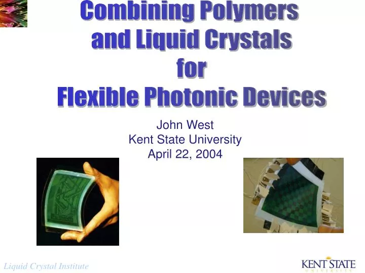
Combining Polymers and Liquid Crystals for Flexible Photonic Devices John West Kent State University April 22, 2004
Outline • Why Flexible • Printed Flexible Cholesteric Displays • Printing techniques • Polymer walls • Stressed Liquid Crystals • Flexible Optical and Electronic Device Manufacturing Facility
Mike Fisch David Heineman Greg R. Novotny Anatoliy Glushenko Ke Zhang Guoqiang(Matt) Zhang Toshihio Aoki Ebru Aylin Buyuktanir Collaborators
Why Flexible?? Rugged Lightweight Roll-to-Roll Manufacturing Cheap Conformable
Approaches to Flexible Displays • Conventional LCD’s and OLED/PLEDS require expensive substrates and development of organic TFT’s • Conventional LCD’s • Use polarized light (non birefringent substrates) • Active matrix (organic TFT’s) • Surface alignment (high temperature and solvent stability) • OLED/PLEDS • Oxygen sensitive (barrier layers) • Active matrix (organic TFT’s) • Unconventional LC Conventional SubstrateApproaches • Polymer Dispersed Liquid Crystals • Bistable Chosterics • Bistable Smectics • Dichroic Dye LCDs
PDLCs: The first flexible display?? Manufactured in a continuous roll-to-roll process Conventional ITO coated polyester substrates (no barrier coatings, no alignment layers) Single pixel.
Bistable Cholesterics • Bright, high contrast images • High resolution with passive matrix • No polarizers required (can use birefringent substrates) • Polymers added for mechanical stability
planar focal conic Reflective Cholesteric Displays Switch between reflecting planar texture and weakly scattering focal conic texture
Switching Mechanism fast homeotropic slow Electric Field transient planar fast focal conic focal conic planar
Figure 1: A four inch square, 320 by 320 pixel bistable cholesteric display made using flexible polyester substrates Flexible Plastic Bistable Cholesteric Display • 4 inch square • 320 x 320 pixel • bistable cholesteric with polymer • flexible polyester substrate West Rouberol, Francl, Ji, Doane and Pfeiffer Asia Display, 1995
Problems • Photolithography makes roll-to-roll processing difficult (expensive) • High polymer content formulation produces light scattering • Reduces reflection in planar state • Increases back scatter in focal conic state • Lowers brightness and contrast
Preliminary Solution • Print resist for etching of electrodes:(roll-to-roll processing) • Segregate polymer into the inter-pixel region: Polymer Walls (bright display)
Wax Transfer Printing of Resist Thermal Print Head Wax Transfer Sheet ITO Coated Polyester Film Tektronix Phaser 240 Wax Transfer Printer
Resist Pattern30 pixels/inch Close-up of the wax pattern printed onto the ITO coated Mylar. The dark lines are the wax pattern. A replica of the wax resist pattern.
Etching and Stripping • Standard etch bath of nitric-sulfuric acid • Strip using warmed (50 C) tetrahydrofuran or toluene
Cell Assembly Top Substrate Bottom Substrate Cholesteric Polymer Mixture BL 094 92% NOA 65 8%
Form Polymer Walls • Improve contrast • Provide rugged displays • Improve the pressure resistance of displays • -- PM-STN-LCDs by Sharp* • Make possible large area, flexible plastic displays • -- adhere the top and bottom substrates • -- maintain uniform thickness * T. Shinomiya, K. Fujimori, S. Yamagishi, K. Nishiguchi, S. Kohzaki, Y. Ishii, F. Funada, and K. Awane, Asia Display, 255 (1995).
Polymer Wall Formation Methods • Photo-mask • -- patterned UV exposure of homogeneous mixtures • of UV-curable monomers and liquid crystals • N. Yamada, S. Kohzaki, F. Funada, and K. Awane, SID Digest of Technical • Papers, 575 (1995). • T. Shinomiya, K. Fujimori, S. Yamagishi, K. Nishiguchi, S. Kohzaki, Y. Ishii, • F. Funada, and K. Awane, Asia Display, 255 (1995). • Y. Ji, J. Francl, W. J. Fritz, P. J. Bos, and J. L. West, SID Digest of Technical • Papers, 611 (1996). • Patterned Electric Field • -- blanket UV exposure after phase separation
Field Formed Polymer Walls • Apply an electric field while solution is warmed aboveclearing/phase separation temperature 2) Cool to RT with field applied to induce polymer segregation 3) UV expose to form polymer walls Kim, Francl, Taheri, West, Appl. Phys. Lett., 72, 2253 (1998).
Field Induced Phase Separation • A patterned electric field is applied to a mixture of liquid crystal and UV curable monomer • Due to a larger dielectric constant, liquid crystal migrates to the high field pixel region while the monomer moves to the low field inter-pixel region • When phase separation is complete, exposure to UV light polymerizes the monomer locking in the wall structure
Electric Field Distribution SEM Image of Polymer Walls
Measure Rate of Field Induced Phase Separation Diagram of Test Cell • One side of cell has aluminum electrodes which block incoming UV light. • Only light passing through inter-pixel makes it to the detector • This allows study of change in concentration of E44 in inter-pixel over time
Absorbance vs Time Mixture of E44 and Trimethylolpropane tris(3-mercaptopropionate) at 40 °C
How T and V Affect the Rate • With the same voltage applied, increasing temperature decreases change observed in absorbance between field on and field off states
Rate of Phase Separation • Occurs in several seconds. • Increasing temperature decreases the magnitude of the effectbut has little effect on the rate. • Increasing the voltage increases the rate and extent of phase separation
Flexible Plastic Display • Compatible with roll-to-roll processing • Uses commercially available materials.
Stressed Liquid Crystals • Developed for beam steering applications • Decouple thickness and speed • Eliminate alignment layers • Fastest nematic devices
F LC polymer Unidirectionally Oriented Micro-Domains of Liquid Crystal Separated by Polymer Network our results AFM image • Middle range of concentration of the polymer: between those for traditional polymer network structures and PDLC. • Well-developed interpenetrating structure of polymer chains and connected liquid crystal domains. • The active area may be of any size • Application of shearing deformation in order to orient the liquid crystal domains SEM image
Effect of Shearing • Reduces the relaxation time of the material. • Decrease the scattering in visible region of spectrum. • The liquid crystal domains become oriented in the direction of shearing • By adjusting the degree of shearing one can control the total phase shift.
Phase retardation shift vs an applied electric field For a 22 m film almost all change of the phase retardation occurs below 130V. The change of phase retardation depends linearly on the applied voltage – simple driving devices
Dynamics of the Relaxation A phase retardation shift of 2 m occurs within 1 ms. Phase retardation of 0.15 m occurred just in40 microseconds
millimeters mm l=l0/nL Possible applications: basic design of an OPA device • Beam steering: a tilted LC director will yield an index of refraction gradient • Industrial application (laser cutting of metals or glass) • Free space communications • Fiber-optics connectors • Military applications • Laser displays • Imaging applications l=l0/nH
SLCs for display applications • 30 volt offset • 10 volt pulse • 20 sec turn on time • 40 sec turn off time
Conclusion • Stressed LC films produce ferroelectric speeds in a nematic film • No alignment layer • No light scattering • No hysteresis • Linear response
The Next StepFlexible Optical and Electronic Device Manufacturing Facility • Wright Capital Grant, $1.6M (State of Ohio) • $1.6M match from industry and KSU • Add to existing Resource Facility • Provide centralized facility for development and prototyping of flexible devices.
Goal • Develop materials required for flexible displays • optimized liquid crystals • organic semiconductors • conducting polymers • optimized substrates • Develop fabrications techniques • printing electrodes • applying thin films • lamination • cutting
Plan Establish a facility for the research and development of flexible electronic devices • Printing • Coating • Lamination • Cutting • Electronics • Materials Synthesis
Planned Research • Evaluation of available substrates • Development of printing techniques for electrodes • Fabrication of printed flexible VGA display using only commercial materials.
Built on an Effective Academic Industrial Collaboration Start-Ups bring Innovation and Jobs HANA Akron Polymer Systems KSU/UA Poly Displays LXD, Inc.
Vision Utilize the unique skills in the region in polymers/liquid crystals and printing to spawn a new industry in flexible displays and related electronic devices.