Download
1 / 20
200 likes | 394 Views
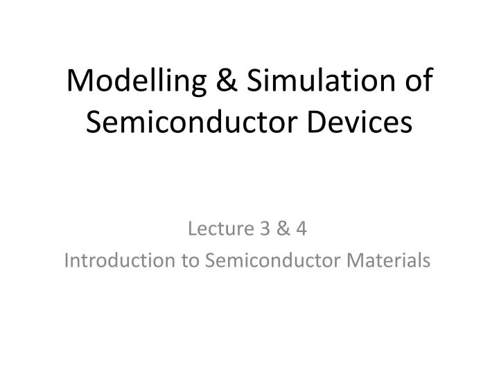
Modelling & Simulation of Semiconductor Devices. Lecture 3 & 4 Introduction to Semiconductor Materials. Prerequisites. To understand this presentation, you should have the following prior knowledge: Draw the structure of an atom, including electrons, protons, and neutrons.

E N D
Modelling & Simulation of Semiconductor Devices Lecture 3 & 4 Introduction to Semiconductor Materials
Prerequisites • To understand this presentation, you should have the following prior knowledge: • Draw the structure of an atom, including electrons, protons, and neutrons. • Define resistance and conductance. • Label an electronic schematic, indicating current flow. • Define Ohm’s and Kirchhoff’s laws. • Describe the characteristics of DC and AC (sine wave) voltages.
Electronic Materials • The goal of electronic materials is to generate and control the flow of an electrical current. • Electronic materials include: • Conductors: have low resistance which allows electrical current flow • Insulators: have high resistance which suppresses electrical current flow • Semiconductors: can allow or suppress electrical current flow
Conductors • Good conductors have low resistance so electrons flow through them with ease. • Best element conductors include: • Copper, silver, gold, aluminum, & nickel • Alloys are also good conductors: • Brass & steel • Good conductors can also be liquid: • Salt water
Copper Atom Conductor Atomic Structure • The atomic structure of good conductors usually includes only one electron in their outer shell. • It is called a valence electron. • It is easily striped from the atom, producing current flow.
Insulators • Insulators have a high resistance so current does not flow in them. • Good insulators include: • Glass, ceramic, plastics, & wood • Most insulators are compounds of several elements. • The atoms are tightly bound to one another so electrons are difficult to strip away for current flow.
Semiconductors • Semiconductors are materials that essentially can be conditioned to act as good conductors, or good insulators, or any thing in between. • Common elements such as carbon, silicon, and germanium are semiconductors. • Silicon is the best and most widely used semiconductor.
Semiconductor Valence Orbit • The main characteristic of a semiconductor element is that it has four electrons in its outer or valence orbit.
Crystal Lattice Structure • The unique capability of semiconductor atoms is their ability to link together to form a physical structure called a crystal lattice. • The atoms link together with one another sharing their outer electrons. • These links are called covalent bonds. 2D Crystal Lattice Structure
Semiconductors can be Insulators • If the material is pure semiconductor material like silicon, the crystal lattice structure forms an excellent insulator since all the atoms are bound to one another and are not free for current flow. • Good insulating semiconductor material is referred to as intrinsic. • Since the outer valence electrons of each atom are tightly bound together with one another, the electrons are difficult to dislodge for current flow. • Silicon in this form is a great insulator. • Semiconductor material is often used as an insulator.
Doping • To make the semiconductor conduct electricity, other atoms called impurities must be added. • “Impurities” are different elements. • This process is called doping.
Semiconductors can be Conductors • An impurity, or element like arsenic, has 5 valence electrons. • Adding arsenic (doping) will allow four of the arsenic valence electrons to bond with the neighboring silicon atoms. • The one electron left over for each arsenic atom becomes available to conduct current flow.
Resistance Effects of Doping • If you use lots of arsenic atoms for doping, there will be lots of extra electrons so the resistance of the material will be low and current will flow freely. • If you use only a few boron atoms, there will be fewer free electrons so the resistance will be high and less current will flow. • By controlling the doping amount, virtually any resistance can be achieved.
Another Way to Dope • You can also dope a semiconductor material with an atom such as boron that has only 3 valence electrons. • The 3 electrons in the outer orbit do form covalent bonds with its neighboring semiconductor atoms as before. But one electron is missing from the bond. • This place where a fourth electron should be is referred to as a hole. • The hole assumes a positive charge so it can attract electrons from some other source. • Holes become a type of current carrier like the electron to support current flow.
Types of Semiconductor Materials • The silicon doped with extra electrons is called an “N type” semiconductor. • “N” is for negative, which is the charge of an electron. • Silicon doped with material missing electrons that produce locations called holes is called “P type” semiconductor. • “P” is for positive, which is the charge of a hole.
Current Flow in N-type Semiconductors • The DC voltage source has a positive terminal that attracts the free electrons in the semiconductor and pulls them away from their atoms leaving the atoms charged positively. • Electrons from the negative terminal of the supply enter the semiconductor material and are attracted by the positive charge of the atoms missing one of their electrons. • Current (electrons) flows from the positive terminal to the negative terminal.
Current Flow in P-type Semiconductors • Electrons from the negative supply terminal are attracted to the positive holes and fill them. • The positive terminal of the supply pulls the electrons from the holes leaving the holes to attract more electrons. • Current (electrons) flows from the negative terminal to the positive terminal. • Inside the semiconductor current flow is actually by the movement of the holes from positive to negative.
In Summary • In its pure state, semiconductor material is an excellent insulator. • The commonly used semiconductor material is silicon. • Semiconductor materials can be doped with other atoms to add or subtract electrons. • An N-type semiconductor material has extra electrons. • A P-type semiconductor material has a shortage of electrons with vacancies called holes. • The heavier the doping, the greater the conductivity or the lower the resistance. • By controlling the doping of silicon the semiconductor material can be made as conductive as desired.
To download this lecture visit http://imtiazhussainkalwar.weebly.com/ End of Lectures 3-4