Download
1 / 25
280 likes | 905 Views
Process Optimization and Development for ZnO Optoelectronics and Photodiodes. Jon Wright Dept. of Materials Science and Engineering, Univ. of Florida, Gainesville, FL Jan 18, 2007. Outline. Introduction & Motivation Background Contacts (Ohmic + Schottky) Ion Implantation (Group V)

E N D
Process Optimization and Development for ZnO Optoelectronics and Photodiodes Jon Wright Dept. of Materials Science and Engineering, Univ. of Florida, Gainesville, FL Jan 18, 2007
Outline • Introduction & Motivation • Background • Contacts (Ohmic + Schottky) • Ion Implantation (Group V) • Project Objectives • Methodology • Preliminary Results • Ir/Au Ohmic Contacts • Surface Treatment Analysis • Conclusions & Timeline
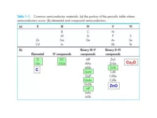
Direct, wide bandgap High excitonic binding energy – 60 meV Inexpensive growth Easily etched (acids and alkalis) Radiation stability ZnO – Basic (Electrical) Properties
ZnO vs. GaN • Bulk ZnO (n-type) commercially available • Grown on inexpensive substrates at low temperatures • Lower exciton energy for GaN • Heterojunction by substitution in Zn-site • Cd ~ 3.0 eV • Mg ~ 4.0 eV • Nanostructures demonstrated • Ferromagnetism at practical Tc when doped with transition metals • Obstacle: good quality, reproducible p-type GaNZnO Bandgap (eV)3.43.2 µe (cm2/V-sec)220200 µh (cm2/V-sec)105-50 me0.27mo0.24mo mh0.8mo0.59mo Exciton binding28 60 energy (meV) Potential Applications UV/Blue optoelectronics Transparent transistors Nanoscale detectors Spintronic devices
Motivation ZnO-based electronic devices • UV light-emitting diodes • Optoelectronics • Transparent thin-film transistors • Flat panel displays • Solar cells • Piezoelectric transducers • Gas-sensors • Photonic devices • High density data storage
Earlier Metallizations Ti/Au, Zn/Au, Al/Pt Re/Ti/Au, Ru, Pt/Ga ρsc 10-3 – 10-7Ω.cm2 c-TLM reduces steps Au ↓ sheet resistance Surface carrier ↑ annealing Adv: oxygen loss Disad: surface degradation Surface cleaning ↓ b Limited info w/ p-ZnO Ohmic contacts to n-ZnO K. Ip et al. AIP (2004).
Schottky Contacts to ZnO • Schottky Obstacles • Surface states • Defects @ surface layer • Metal/ZnO intermixing • Typically Au, Ag, Pd, Pt • Φb ~ 0.6-0.84 eV • n > 1 (~1-2+) • Poor thermal stability • High n factor • Tunneling • Interface layer • Surface conductivity • Deep recomb. centers
p-type Doping in ZnO • Several deposition methods • Group V: N, P, As, Sb – all on O sites • MBE requires low temp for high dopant conc. • Crystal quality poor below 500°C • Post-deposition annealing results inconsistent • Hole conc. ~ 1015-1017 cm-3 • Limitations in band edge electroluminescence • Deep traps: non-radiative recombination centers • Low density of holes at junction • Diffusion of carriers away from active region
p-type Ion Implantation for ZnO • Dopant beam makes vacancies for acceptors • Questions: • Correct ion dosage • Limiting residual damage • Maximizing acceptors • Need for understanding • Damage accumulation • Thermal stability of defects
Project Objectives The goals of this project are three fold: • Optimization of Ohmic contacts to ZnO • Ir, Re, WNx, TiNx, ZrNx, and TaNx • Optimization of Schottky contacts to ZnO • Ir, Re, WNx, TiNx, ZrNx, and TaNx • Investigation of electrical properties for implanted Group V dopants in ZnO Aim: Develop processes for ZnO devices • Specifically for UV optoelectronics and LEDs • Realization of p-type ZnO nanowire devices
Why Use These Materials? • Nitrides have excellent electrical properties • Highly conductive • High melting temperature • Strong bonds lead to low diffusivity probability • Thermally stable – some Nitrides up to 800°C on GaN • Ir, Re successful novel metallizations for GaN • Superb thermal stability • Group V elements most promising p-type dopants • Difficulty with shallow acceptor levels due to defect states • Group I elements tend to occupy interstitial sites (act as donors)
Methodology – Ohmic Contacts Processing • Surface Treatment/Cleaning • Photolithography – c-TLM pattern if possible [J. Chen thesis] • Sputter deposit metallization scheme • Novel metallizations include Au overlayer • Lift-off • Anneal (300°C-1000°C, 1 min, N2 or O2)
Methodology – Schottky Contacts Processing • Sample Treatment/Cleaning • Photolithography for Ohmic contact (outer ring) • Sputter deposit Ti/Au (basic Ohmic contact) • Lift-off • RTA anneal 450°C , 30 sec N2 ambient • Schottky photolithography realignment • Sputter deposit metallization scheme • Novel metallizations include Au overlayer • Lift-off • Anneal contacts (300°C-1000°C, 1 min, N2 or O2)
Methodology – Contact Measurements • Electrical Characterization • Contact resistance • 4-probe TLM measurement • 2-probe C-TLM measurement • ΔAnnealing temperature • ΔAnnealing time • Variation in measurement temperature (RT – 300°C) • Schottky Diode parameter measurements • Auger Electron Spectroscopy • Scanning Electron Microscopy • Thermal stability measurements
Methodology – Ion Implantation • N, P, As dopants @ doses 1013-1014 cm-2 • Implantation temp varied RT – 300°C • Annealed between 600 – 950°C • RTA • PLD chamber, O2 ambient (in-situ) • Hall measurements used to calculate: • Carrier type • Carrier density • Acceptor ionization energy • Use of Oxygen to reduce vacancies • Depth Profiles by AES/SIMS
Ion Implantation → ZnO Nanowires • Ability to create pn junction is paramount • Acceptor implantation + characterization • Why Nanowires? • FETs, photodetectors, gas sensors, nano-cantilevers • Allow investigation of carrier transport properties (1-D) • Surface quality, ambient environment critical to character of device • ZnO nanorods (d ~130 nm) grown by MBE • p-type nanowires by injection of acceptors • Contacts on wires using p-type Ohmic metals • Nanowire pn junctions • Masked implantation OR focused ion beam • Determination of EA, ρ – activation kinetics
Ir/Au Contacts – AES Profiles Only slight intermixing btw Au and Ir layers until 800°C(+)
Ir/Au Contacts – Thermal Stability Pre-anneal No change to Rsh after 30 days 30 Days
Ir/Au Contacts – N2 vs. O2 Anneal Resistance increased w/ O2 anneal – IrO2 layer
Ir/Au Contacts – N2 vs. O2 Anneal AES can not detect IrO2 layer, however more interdiffusion of Ir w/ N2 anneal
Surface Treatment – IV Character All treatments result in Ohmic contacts except for Oxygen plasma.
Acknowledgements • Advisory Committee • Prof. S.J. Pearton (Chair) • Prof. C.R. Abernathy • Prof. D.P. Norton • Prof. R. Singh • Prof. F. Ren • Contributors • Dr. L. Stafford, Dr. B.P. Gila, L.F. Voss, R. Khanna, H-T. Wang, S. Jang