Download
1 / 3
30 likes | 188 Views
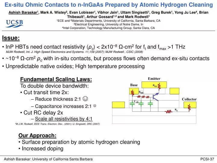
Issue: InP HBTs need contact resistivity ( ρ c ) < 2x10 −8 Ω-cm 2 for f t and f max >1 THz MJW Rodwell, Int. J. High Speed Electronics and Systems. 11,159 (2007); MJW Rodwell , CSIC (2008) ~10 −8 Ω-cm 2 ρ c with in-situ contacts, but process flows often demand ex-situ contacts

E N D
Issue: InP HBTs need contact resistivity (ρc) < 2x10⁻⁸ Ω-cm2 for ft and fmax >1 THzMJW Rodwell, Int. J. High Speed Electronics and Systems. 11,159 (2007); MJW Rodwell , CSIC (2008) ~10−8 Ω-cm2ρc with in-situ contacts, but process flows often demand ex-situ contacts Unpredictable native oxides; High temperature processing Ex-situ Ohmic Contacts to n-InGaAs Prepared by Atomic Hydrogen Cleaning • Fundamental Scaling Laws: • To double device bandwidth: • Cut transit time 2x: • Reduce thickness 2:1 ☺ • Capacitance increases 2:1 ☹ • Cut RC delay 2x • Scale all resistivities by 4:1 *M.J.W. Rodwell, IEEE Trans. Electron. Dev., (2001); U. Singisetti, DRC (2007) Ashish Baraskar1, Mark A. Wistey3, Evan Lobisser1, Vibhor Jain1, Uttam Singisetti1, Greg Burek1, Yong Ju Lee4, Brian Thibeault1, Arthur Gossard1,2 and Mark Rodwell1 1ECE and 2Materials Departments, University of California, Santa Barbara, CA 3Electrical Engineering, University of Notre Dame, In 4Intel Corporation, Technology Manufacturing Group, Santa Clara, CA • Our Approach: • Surface preparation by atomic hydrogen cleaning • Increased doping Ashish Baraskar: University of California Santa Barbara PCSI-37
Ex-situ Ohmic Contacts to n-InGaAs Prepared by Atomic Hydrogen Cleaning 20 nm Mo 100 nm In0.53Ga0.47As (n-doped) 100 nm In0.52Al0.48As (NID) InP (semi-insulating) • Experimental Details: • Highly doped n-In0.53Ga0.47As by solid source MBE • Surface exposed to air • Atomic hydrogen cleaning in MBE • Surface observed under RHEED before metal deposition • Transmission Line Model (TLM) for contact resistance measurement Contact metal: Molybdenum (Mo) Experimental Results with Mo Contact Metal • Electron concentration, n = 5x1019 cm-3 • Mobility, µ = 770 cm2/Vs • Sheet Resistance, Rsh = 15 ohm/□ (100 nm thick film) Hcleaned (MBE) contacts are comparable to in-situ contacts Ashish Baraskar: University of California Santa Barbara PCSI-37
Ex-situ Ohmic Contacts to n-InGaAs Prepared by Atomic Hydrogen Cleaning • Conclusions: • Atomic hydrogen effectively cleans air-exposed semiconductor surfaces • ρc ~ (1.3 ± 0.5) Ω-µm2 for atomic hydrogen cleaned Mo-nInGaAs contacts • Contact resistivity comparable to in-situ Mo-nInGaAs contacts • Mo contacts are thermally stable on InGaAs up to 400 oC • Contacts suitable for THz transistors Poster No: We1645 Acknowledgements ONR, DARPA-TFAST, DARPA-FLARE • Thermal Stability: • Contacts annealed under N2 flow at 300 and 400 oC for 1 minute duration • Low resistivity maintained after anneal: (1.3 ± 0.5) × 10-8 Ω-cm2 Ashish Baraskar: University of California Santa Barbara PCSI-37