Download
1 / 2
20 likes | 111 Views
Detection of Structure and Electrical Level of Point Defects in Semi-Insulating SiC M. E. Zvanut, University of Alabama at Birmingham, DMR-0506069.

E N D
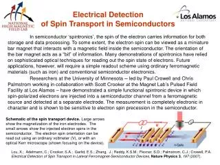
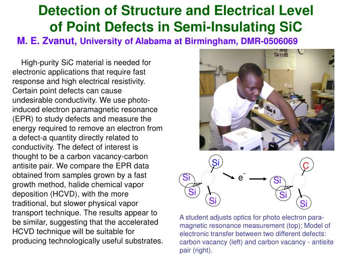
Detection of Structure and Electrical Level of Point Defects in Semi-Insulating SiC M. E. Zvanut, University of Alabama at Birmingham, DMR-0506069 High-purity SiC material is needed for electronic applications that require fast response and high electrical resistivity. Certain point defects can cause undesirable conductivity. We use photo-induced electron paramagnetic resonance (EPR) to study defects and measure the energy required to remove an electron from a defect-a quantity directly related to conductivity. The defect of interest is thought to be a carbon vacancy-carbon antisite pair. We compare the EPR data obtained from samples grown by a fast growth method, halide chemical vapor deposition (HCVD), with the more traditional, but slower physical vapor transport technique. The results appear to be similar, suggesting that the accelerated HCVD technique will be suitable for producing technologically useful substrates. Si C Si e- Si Si Si Si Si A student adjusts optics for photo electron para-magnetic resonance measurement (top); Model of electronic transfer between two different defects: carbon vacancy (left) and carbon vacancy - antisite pair (right).
Detection of Structure and Electrical Level of Point Defects in Semi-Insulating SiC M. E. Zvanut, University of Alabama at Birmingham, DMR 0506069 Undergraduates acquire research experience including: ● basic spectroscopy techniques ● sample cleaning and annealing procedures ● importance of growth and post-growth environment on the number of defects Undergraduate physics major gets ‘hands on’ experience using the tools of electron paramagnetic resonance, optics, and annealing. This student is doing research for her Advanced Laboratory course, which will ultimately result in the presentation of a university proposal.