Download
1 / 16
160 likes | 168 Views
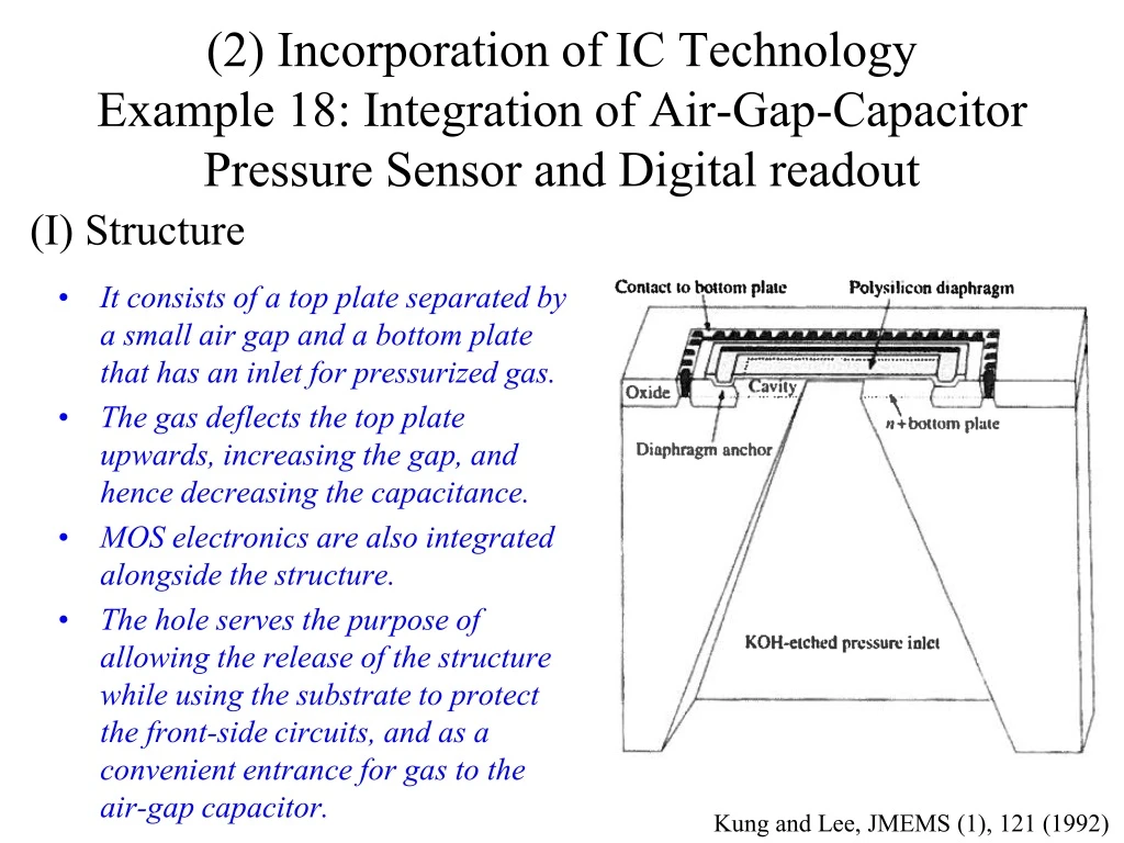
(2) Incorporation of IC Technology Example 18: Integration of Air-Gap-Capacitor Pressure Sensor and Digital readout. (I) Structure. It consists of a top plate separated by a small air gap and a bottom plate that has an inlet for pressurized gas.

E N D
(2) Incorporation of IC TechnologyExample 18: Integration of Air-Gap-Capacitor Pressure Sensor and Digital readout (I) Structure • It consists of a top plate separated by a small air gap and a bottom plate that has an inlet for pressurized gas. • The gas deflects the top plate upwards, increasing the gap, and hence decreasing the capacitance. • MOS electronics are also integrated alongside the structure. • The hole serves the purpose of allowing the release of the structure while using the substrate to protect the front-side circuits, and as a convenient entrance for gas to the air-gap capacitor. Kung and Lee, JMEMS (1), 121 (1992)
(II) Process • After nMOS processing up to patterning and etching of the poly-Si gates, re-oxidation, and junction drive-in of the source/drain regions. • After deposition and patterning of LPCVD Si nitride layer. • After boro-phosphosilicate glass (BPSG) deposition, flow/anneal, and trench cut for the diaphragm anchor. Kung and Lee, JMEMS (1), 121 (1992)
(II) Process (cntd.) (d) LPCVD deposition of 1 mm of poly-Si, P-doping, glass wet etch, poly-Si patterning, and etching. (e) After contact cuts, aluminum-1% Si sputter deposition, and sinter Kung and Lee, JMEMS (1), 121 (1992)
(III) Back-Side process (a) After IR alignment for backside nitride paterning/etching, and one-sided KOH etch. (b) After one-sided concentrated HF etch. Kung and Lee, JMEMS (1), 121 (1992)
Key process parameters. Kung and Lee, JMEMS (1), 121 (1992)
(IV) Sensor Architecture • Charge-redistribution sensing is used to discern the capacitive change in the sense capacitor relative to an identical reference capacitor. • The sense capacitor gets charged and discharged onto the reference capacitor; any capacitive difference in the two manifests itself as a voltage proportional to this difference. • On chip components are the air-gap capacitors, MOS switches, and nMOS preamplifier. Kung and Lee, JMEMS (1), 121 (1992)
Example 19: Gap Comb-Drive Resonant Actuator Top view of the resonator SEM photograph of the resonantor Hirano etal., JMEM (1), 52 (1992)
Process • Film deposition. • After RIE of poly-Si. • After thermal oxidation. • Released actuator. Hirano etal., JMEM (1), 52 (1992)
SEM close up of the electrodes Hirano etal., JMEM (1), 52 (1992)
Adhesion Problems in Surface Micromachining • After sacrificial layer removal, the wafers are normally rinsed in DI water and dried. • Surface tension of the water under the structures pulls them down to the surface of the wafer, and in some cases causes them to stick to the surface of the water permanently. • This problem can be avoided by using thick structural and sacrificial layers; however, this is only possible when the design allows thick layers to be used.
Adhesion Prevention • If long or thin plates and beams are necessary, there are several options for preventing adhesion. • One is to place small pumps on the bottom surface of the plates to give them a tendency to pull back off the substrate. • If the spacing of the pumps (known as dimples) is close enough, the central (flat) portion of the plate will in fact never touch the substrate. • This critical spacing is a function of the structural and sacrificial layers. For 2 mm layers the minimum dimple spacing is calculated to be ~ 50 mm.
There are several ways to avoid adhesion, which are all focused on avoiding surface tension. • Freeze drying (sublimation) of the final rinsing solution, e.g., DI water. • Using an integrated polymer support structure during release etching, then ashing in oxygen plasma. • Gradually replacing acetone with photoresist, then spinning and ashing the resist.
Adhesion Prevention (cntd.) • To avoid adhesion the micromachined structure may be prevented from coming in contact with the surface during the wet etching. • One way to accomplish this is through adding polymer (e. g.,xylylene) supports to the structure before the release etch, then ashing the polymer a dry oxygen plasma after release and drying.
Bulk vs. surface Micromachining • Bulk • Advantages • Well established; well characterized materials; Rugged structure; Larger masses (accelerometers); Larger areas (capacitive sensors); Higher piezoresistive gauge factor • Disadvantages • Large die areas (expensive); somewhat limited structure geometries; Not compatible with IC technology; Not easily amenable to standard cell design.
Surface • Advantages • Rugged structure (works for vibrations and shocks); Small die areas (cheap); Compatible with IC technology (surface structures) • Disadvantages • Fragile structures ( especially with respect to contact); smaller masses and smaller areas and both tend to degrade sensitivity.