Download
1 / 57
580 likes | 593 Views
Digital Binary Logic. Brief History of Digital Electronics. Digital electronics can be found in many applications in the form of microprocessors, microcontrollers, PCs, DSPs, and an uncountable number of other systems. The historic development of design of digital circuits:

E N D
Brief History of Digital Electronics • Digital electronics can be found in many applications in the form of microprocessors, microcontrollers, PCs, DSPs, and an uncountable number of other systems. • The historic development of design of digital circuits: • resistor-transistor logic (RTL) • diode-transistor logic (DTL) • transistor-transistor logic (TTL) • emitter-coupled logic (ECL) • NMOS • complementary MOS (CMOS)
Digital Binary Logic • Digital electronics represent signals by discrete bands of analog levels, rather than by a continuous range.
Digital Binary Logic • Digital electronics represent signals by discrete bands of analog levels, rather than by a continuous range. • All levels within a band represent the same signal state. • Small changes to the analog signal levels due to manufacturing tolerance, or noise do not leave the discrete envelope, and as a result are ignored by signal state sensing circuitry.
Digital Binary Logic • Digital electronics represent signals by discrete bands of analog levels, rather than by a continuous range. • All levels within a band represent the same signal state. • Small changes to the analog signal levels due to manufacturing tolerance, or noise do not leave the discrete envelope, and as a result are ignored by signal state sensing circuitry. • Binary logic is the most common style of digital logic. • The signal is either a 0 (low, false) or a 1 (high, true) - Positive Logic Convention
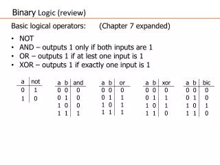
Digital Binary Logic • Digital electronics represent signals by discrete bands of analog levels, rather than by a continuous range. • All levels within a band represent the same signal state. • Small changes to the analog signal levels due to manufacturing tolerance, or noise do not leave the discrete envelope, and as a result are ignored by signal state sensing circuitry. • Binary logic is the most common style of digital logic. • The signal is either a 0 (low, false) or a 1 (high, true) - Positive Logic Convention • Mathematical representation of logical operations is Boolean algebra: set of operations (NOT, AND, OR, NAND, NOR, etc.) with binary or logical elements. • To perform general logical operations, a logic family must contain NOT and at least one another function of two inputs OR or AND.
Logic Gate Symbols and Boolean Expressions • A logic gate is a physical model of a Boolean function: it performs a logical operation on one or more logic inputs and produces a single logic output.
Logic Gates: AND The simples gates are AND and OR. They can be built from switches or using the simplest form of electronic logic - diode logic. A = 0 , B = 0 both diodes are forward biased both diodes conduct out is LOW 0.
Logic Gates: AND The simples gates are AND and OR. They can be built from switches or using the simplest form of electronic logic - diode logic. A = 0 , B = 0 both diodes are forward biased both diodes conduct out is LOW 0. A = 0 , B = 1 DB is reverse biased does not conduct, DA is forward biased conducts out is LOW 0.
Logic Gates: AND The simples gates are AND and OR. They can be built from switches or using the simplest form of electronic logic - diode logic. A = 0 , B = 0 both diodes are forward biased both diodes conduct out is LOW 0. A = 0 , B = 1 DB is reverse biased does not conduct, DA is forward biased conducts out is LOW 0. A = 1 , B = 0 DA is reverse biased does not conduct, DB is forward biased conducts out is LOW 0.
Logic Gates: AND The simples gates are AND and OR. They can be built from switches or using the simplest form of electronic logic - diode logic. A = 0 , B = 0 both diodes are forward biased both diodes conduct out is LOW 0. A = 0 , B = 1 DB is reverse biased does not conduct, DA is forward biased conducts out is LOW 0. A = 1 , B = 0 DA is reverse biased does not conduct, DB is forward biased conducts out is LOW 0. A = 1 , B = 1 both diodes are reverse biased both the diodes do not conduct out is HIGH 1.
Logic Gates: OR A = 0 , B = 0 both diodes are reverse biased does not conduct out is LOW 0. A = 0 , B = 1 DA is reverse biased does not conduct, DB is forward biased conducts out is HIGH 1. A = 1 , B = 0 DB is reverse biased does not conduct, DA is forward biased conducts out is HIGH 1. A = 1 , B = 1 both diodes are reverse biased both the diodes conduct out is HIGH 1.
Logic Gates: NAND & NOR • The simple diode logic allows AND and OR, but not inverters an incomplete form of logic. • Also, without some kind of amplification it is not possible to have such basic logic operations cascaded as required for more complex logic functions.
Logic Gates: NAND & NOR • The simple diode logic allows AND and OR, but not inverters an incomplete form of logic. • Also, without some kind of amplification it is not possible to have such basic logic operations cascaded as required for more complex logic functions. • However, any gate can be built from NAND or NOR gates. This enables a circuit to be built from just one type of gate, either NAND or NOR. • To build NAND or NOR inverter is required transistors needed.
Logic Gates: NAND & NOR • The simple diode logic allows AND and OR, but not inverters an incomplete form of logic. • Also, without some kind of amplification it is not possible to have such basic logic operations cascaded as required for more complex logic functions. • However, any gate can be built from NAND or NOR gates. This enables a circuit to be built from just one type of gate, either NAND or NOR. • To build NAND or NOR inverter is required transistors needed. • Conclusion. • To build a functionally complete logic systems transistors are used. • The most basic digital building block is the inverter.
Diode-Transistor Logic (DTL) Gate • The inversion and level-restoration problem associated with diode logic can be solved by adding a diode and transistor to form the diode-transistor logic (DTL) gate • It will be analyzed in detail sin Chapter 9; here is a brief overview.
Diode-Transistor Logic (DTL) Gate • The inversion and level-restoration problem associated with diode logic can be solved by adding a diode and transistor to form the diode-transistor logic (DTL) gate • It will be analyzed in detail, there is a brief overview. On the left, diodes D1 and D2 are both off, whereas D3 and Q1 are on. Node 1 is at1.3 V: V1 = VD3 + VBE = 0.6 V + 0.7 V = 1.3 V The current I through resistor RB and diode D3 becomes the base current IB of transistor Q1. The value of IB is designed to cause Q1 to saturate so thatvO = VCESAT (for example, 0.05 to 0.1 V).
Diode-Transistor Logic (DTL) Gate • The inversion and level-restoration problem associated with diode logic can be solved by adding a diode and transistor to form the diode-transistor logic (DTL) gate • It will be analyzed in detail,here is a brief overview. On the right, input B is now at 0 V, corresponding to a logical 0. Diode D2 is conducting, holding node 1 at 0.6 V. Now diode D3 and transistor Q1 must both be off, because the voltage at node 1 is now less than the two diode voltage drops required to turn on both D3 and Q1. The base current of Q1 is now zero; Q1 will be off with IC = 0, and the output voltage will be at +3.3 V, corresponding to a logical 1. A similar situation holds for the circuit if both inputs are low.
Diode-Transistor Logic (DTL) Gate • The inversion and level-restoration problem associated with diode logic can be solved by adding a diode and transistor to form the diode-transistor logic (DTL) gate • It will be analyzed in detail, here is a brief overview. On the left, diodes D1 and D2 are both off, whereas D3 and Q1 are on. Node 1 is at1.3 V: V1 = VD3 + VBE = 0.6 V + 0.7 V = 1.3 V The current I through resistor RB and diode D3 becomes the base current IB of transistor Q1. The value of IB is designed to cause Q1 to saturate so thatvO = VCESAT (for example, 0.05 to 0.1 V). On the right, input B is now at 0 V, corresponding to a logical 0. Diode D2 is conducting, holding node 1 at 0.6 V. Now diode D3 and transistor Q1 must both be off, because the voltage at node 1 is now less than the two diode voltage drops required to turn on both D3 and Q1. The base current of Q1 is now zero; Q1 will be off with IC = 0, and the output voltage will be at +3.3 V, corresponding to a logical 1. A similar situation holds for the circuit if both inputs are low.
The Ideal Inverter The ideal inverter has the following voltage transfer characteristic (VTC) and is described by the following symbol ?
The Ideal Inverter The ideal inverter has the following voltage transfer characteristic (VTC) and is described by the following symbol V+ and V- are the supply rails VH and VL describe the high and low logic levels at the output
Inverter - circuit An inverter operating with power supplies at V+ and 0 V can be implemented using a switch with a resistive load. ? MOSFET
Inverter - circuit An inverter operating with power supplies at V+ and 0 V can be implemented using a switch with a resistive load. ? Q-point
Inverter - circuit An inverter operating with power supplies at V+ and 0 V can be implemented using a switch with a resistive load. Q-point
Inverter - circuit An inverter operating with power supplies at V+ and 0 V can be implemented using a switch with a resistive load.
Logic Gate Design Goals • An ideal logic gate is highly nonlinear and attempts to quantize the input signal to two discrete states. In an actual gate, the designer should attempt to minimize the undefined input region while maximizing noise margins
Logic Gate Design Goals • An ideal logic gate is highly nonlinear and attempts to quantize the input signal to two discrete states. In an actual gate, the designer should attempt to minimize the undefined input region while maximizing noise margins • The logic gate is unidirectional. Changes at the output should have no effect on the input.
Logic Gate Design Goals • An ideal logic gate is highly nonlinear and attempts to quantize the input signal to two discrete states. In an actual gate, the designer should attempt to minimize the undefined input region while maximizing noise margins • The logic gate is unidirectional. Changes at the output should have no effect on the input. • Voltage levels at the output of one gate should be compatible with the input levels of a following gate
Logic Gate Design Goals • An ideal logic gate is highly nonlinear and attempts to quantize the input signal to two discrete states. In an actual gate, the designer should attempt to minimize the undefined input region while maximizing noise margins • The logic gate is unidirectional. Changes at the output should have no effect on the input. • Voltage levels at the output of one gate should be compatible with the input levels of a following gate • The output of one gate should be capable of driving the input of more than one gate: the gate should have sufficient fan-out and fan-in capabilities
Logic Gate Design Goals • An ideal logic gate is highly nonlinear and attempts to quantize the input signal to two discrete states. In an actual gate, the designer should attempt to minimize the undefined input region while maximizing noise margins • The logic gate is unidirectional. Changes at the output should have no effect on the input. • Voltage levels at the output of one gate should be compatible with the input levels of a following gate • The output of one gate should be capable of driving the input of more than one gate: the gate should have sufficient fan-out and fan-in capabilities • The gate should consume minimal power (and area for ICs) and still operate under the design specifications
Dynamic Response of Logic Gates • An important characteristic of the logical gates is the response in the time domain • To describe the typical pulse signal at the input, we introduce: • The rise and fall times: tf and tr, are measured at the 10% and 90% points on the transitions between the two states as shown by the following expressions: • V10% = VL + 0.1V • V90% = VL + 0.9V = VH – 0.1V • where V is the logic swing given by V = VH - VL
Dynamic Response of Logic Gates • For the input on the top, will the output will be like the signal on the bottom plot?
Dynamic Response of Logic Gates • For the input on the top, will the output will be like the signal on the bottom plot? • No, It will be delayed.
Dynamic Response of Logic Gates • For the input on the top, will the output will be like the signal on the bottom plot? • No, It will be delayed. • Propagation delay describes the amount of time between the input reaching the 50% point and the output reaching the 50% point. The 50% point is described by the following: • The high-to-low propagation delay, PHL, and the low-to-high propagation delay, PLH, are usually not equal, but can be combined as an average value:
NMOS Inverter with a Resistive Load • The basic inverter circuit consists of an NMOS switching device MS and a resistor load element. • MS is the switching transistor used to “pull” the output high - toward to the power supply VDD • The resistor R is used to “pull” the output low, to force vOto VL • The size of R and the W/L ratio of MS are the design factors that need to be chosen.
NMOS Inverter with a Resistive Load When the input voltage is at a low state, vI = VL , MS should be cut off, with iD = 0, so that vO = VDD = VH Thus, in this particular logic circuit, the value of VHis set by the power supply voltage VDD = 2.5V. To ensure that switching transistor MS is cut off when the input is in the low logic state, VLis designed to be 25 to 50 percent of the threshold voltage VTNof switch MS. This choice alsoprovides a reasonable value for noise margin NML . The equation for the output voltage (load line): vO = vDS = VDD − iD R
NMOS Inverter with a Resistive Load When the input voltage is at a low state, vI = VL , MS should be cut off, with iD = 0, so that vO = VDD = VH Thus, in this particular logic circuit, thevalue of VHis set by the power supplyvoltage VDD = 2.5V. To ensure that switching transistor MS is cut off when the input is in the low logic state, VLis designed to be 25 to 50 percent of the threshold voltage VTNof switch MS. This choice alsoprovides a reasonable value for noise margin NML . The equation for the output voltage (load line): vO = vDS = VDD − iD R When the input voltage is at a high state, vI = VH , switch MS is set in the triode region by the design of W/L parameter and load line to ensure that vO = VL.
NMOS with Resistive LoadDesign Example (1) • Design a NMOS resistive load inverter for • VDD = 3.3 V • P = 0.1 mW when VL = 0.2 V • Kn = 60 A/V2 • VTN = 0.75 V • Find the value of the load resistor R and the W/L ratio of the switching transistor MS
NMOS with Resistive LoadDesign Example (2) • First the value of the current through the resistor (for vO= VL) must be determined by using the following: • The value of the resistor can now be found by the following, which assumes that the transistor is on and the output is low:
NMOS with Resistive LoadDesign Example (3) • For vI = VH = 3.3 V, and vO = VL = 0.2V, the transistor’s drain-source voltage VDS =VL will be less than VGS-VTN=VH-VTN • Therefore it will be operating in the triode region. Using the triode region equation for the MOSFET, the W/L ratio can be found:
PMOS Logic • PMOS logic circuits predated NMOS logic circuit, but were replaced since they operate at slower speeds Resistive Load Saturated Load Linear Load Depletion-Mode Load Pseudo PMOS
Transistor-Transistor Logic TTL NJIT ECE271 Dr.Serhiy Levkov