Download
1 / 9
110 likes | 285 Views
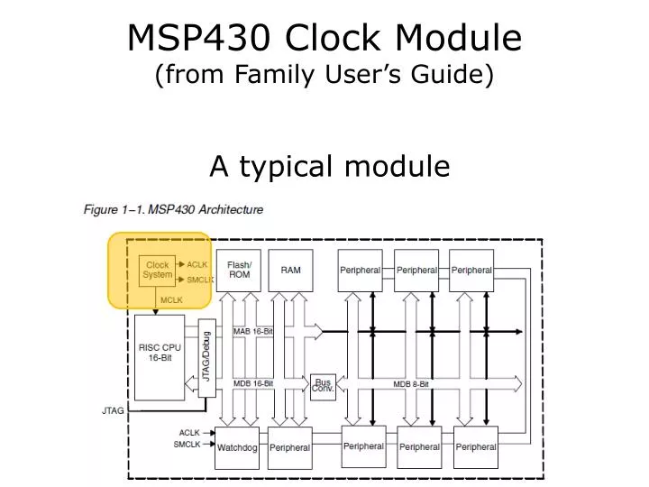
MSP430 Clock Module (from Family User’s Guide). A typical module. Clock Module. What do control bits do?. Where do control bits reside?. DCO (Digitally Controlled Oscillator). DCO Registers. Readable, writeable, initial value=0. DCOCTL = 0xD3; // C code to set DCOCTL.

E N D
MSP430 Clock Module(from Family User’s Guide) A typical module
Clock Module What do control bits do? Where do control bits reside?
DCO Registers Readable, writeable, initial value=0 DCOCTL = 0xD3; // C code to set DCOCTL.
Use predefined constants in code /* Basic Clock System Control 2 * SELM_0 -- DCOCLK * DIVM_0 -- Divide by 1 * ~SELS -- DCOCLK * DIVS_0 -- Divide by 1 * ~DCOR -- DCO uses internal resistor */ BCSCTL2 = SELM_0 + DIVM_0 + DIVS_0; … #define SELM0 (0x40) /* MCLK Source Select 0 */ #define SELM1 (0x80) /* MCLK Source Select 1 */ #define DIVS_0 (0x00) /* SMCLK Divider 0: /1 */ #define DIVS_1 (0x02) /* SMCLK Divider 1: /2 */ #define DIVS_2 (0x04) /* SMCLK Divider 2: /4 */ #define DIVS_3 (0x06) /* SMCLK Divider 3: /8 */ #define DIVM_0 (0x00) /* MCLK Divider 0: /1 */ #define DIVM_1 (0x10) /* MCLK Divider 1: /2 */ #define DIVM_2 (0x20) /* MCLK Divider 2: /4 */ #define DIVM_3 (0x30) /* MCLK Divider 3: /8 */ #define SELM_0 (0x00) /* MCLK Source Select 0: DCOCLK */ #define SELM_1 (0x40) /* MCLK Source Select 1: DCOCLK */ #define SELM_2 (0x80) /* MCLK Source Select 2: XT2CLK/LFXTCLK */ #define SELM_3 (0xC0) /* MCLK Source Select 3: LFXTCLK */ … But be careful or… BCSCTL2 = 0x00; // Comment this well!
Use predefined constants (cont’d) /* Follow recommended flow. First, clear all DCOx and MODx bits. Then * apply new RSELx values. Finally, apply new DCOx and MODx bit values. */ DCOCTL = 0x00; BCSCTL1 = CALBC1_16MHZ; /* Set DCO to 16MHz */ DCOCTL = CALDCO_16MHZ; /* Basic Clock System Control 1 * XT2OFF -- Disable XT2CLK * ~XTS -- Low Frequency * DIVA_0 -- Divide by 1 */ BCSCTL1 |= XT2OFF + DIVA_0; /* Basic Clock System Control 3 * XT2S_0 -- 0.4 - 1 MHz * LFXT1S_2 -- If XTS = 0, XT1 = VLOCLK ; If XTS = 1, XT1 = 3 - 16-MHz crystal or resonator * XCAP_1 -- ~6 pF */ BCSCTL3 = XT2S_0 + LFXT1S_2 + XCAP_1;