Download
1 / 43
430 likes | 557 Views
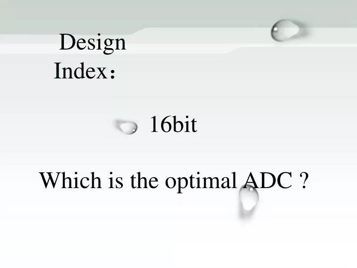
Design Index :. 16bit. Which is the optimal ADC ?. Incremental Data Converter. Date : 2013.03.30. Reporter : Sihai Chen. TJIC Design Center Battery Management. Introduction. 1. Incremental data converter.

E N D
Design Index: 16bit Which is the optimal ADC ?
Incremental Data Converter Date:2013.03.30 • Reporter: SihaiChen TJIC Design Center Battery Management
Introduction 1 Incremental data converter 2 Extensions of First-order Converter 3 Properties of IDC 4 Design Example 5 Contents
Introduction ADC is extensively used. Table 1.1 A/D converter requirements of different applications
Introduction • Application requirements: • high resolution • high speed • simple hardware • low power- and area-consumption • insensitivity of environmental effects • High resolution limitations • analog elements matching • switching-noise
Introduction Table 1.2 Classification of different A/D converter architecture
Introduction • Characteristics of IDC • Converter speed to resolution • Insensitivity of analog elements matching • High resolution • Low~Med bandwidth • Various architectures to make trade-off • Good performance for dc measurements • sensitive to offset, linearity, stability
Incremental Data Converter • 1978, Plassche introduced the structure of first-order incremental data converter for the first time. • 1985, Robert and Valencic introduced a similar structure with more theoretical details in a low-voltage CMOS environment, naming the converter “incremental A/D converter”. • 2004, Markus introduced the modified IDC, and clearly explained the theory and applications of IDC, naming “incremental ΔΣ converter”.
Incremental Data Converter • First-order incremental A/D converter • A hybrid between dual-slope converter and ΔΣ one Figure2.1 Block diagram of the Dual-Slope converter
Incremental Data Converter • First-order incremental A/D converter • A hybrid between dual-slope converter and ΔΣ one Figure2.2 Block diagram of the first-order ΔΣconverter
Incremental Data Converter • First-order incremental A/D converter • A hybrid between dual-slope converter and ΔΣ one Figure2.3 Block diagram of the Dual-Slope converter
Incremental Data Converter • How dual-slope A/D works Two-cycle mode: First-cycle Second-cycle So, there is Question1:How to enhance the resolution of Dual-slope A/D converter?(Clue: ε=?) Note:
Incremental Data Converter • How First-order IDC works At the (N+1)thsampling, Obviously, After , (*) Vin∈(0, Vref), -Vref=0; Vin∈(-Vref,Vref), -Vref= -VrefTo be easily understand, -Vref=0.
Incremental Data Converter • In an ideal A/D converter, • Rearranging Eq.(*), • That is, Question2:How to enhance the resolution of incremental A/D converter? Conclusion:
Incremental Data Converter • For the Bipolar operation, (Vin∈(-Vref,Vref),-Vref= -Vref) • after N cycles, • and ,
Extensions of First-order Converter • The key requirements of extensions: • Fast • High resolution • Actually, it means: (3-1)
Extensions of First-order Converter • Depending on the Eq.(3-1), • α=1, β>0,b>0; • Refining the Quantization Noise (or extended counting conversion) • 0<α< 1, β=0,b=0; • Different Architecture • High-order Modulators
Extensions of First-order Converter • Refining the Quantization Noise • First-order IDC • Refine the residual signal High nbitbit Low nRbit error
Extensions of First-order Converter • Optimal Architecture First-order IDC(3~5bit) + Cyclic(8~10bit)
Extensions of First-order Converter • Optimal Architecture First-order IDC(3~5bit) + Cyclic(8~10bit)
Extensions of First-order Converter • Other Architectures • Multi-bit ADC Refine the quantization in every cycle • Two-steps algorithmic conversion First step: MSB nbit/2 Second step: LSB nbit/2 Total cycles:
Extensions of First-order Converter • Refine the Quantization Noise • First-order IDC • CIFF High-order IDC • Dual-slope converter • Single-slope converter • Cyclic converter • SAR converter • Flash(Pipeline) converter
Extensions of First-order Converter • Refine the Quantization Noise
Extensions of First-order Converter • Different Architecture • MASH(multi-stage noise shaping)
Extensions of First-order Converter • High-order Modulator • To be easily understand, here is a simple architecture. • Low-distortion CIFF second-order IDC
Extensions of First-order Converter • How it works Given the reset signal, V1[0]= V2[0]=0. Time-Domain Z-Domain
Extensions of First-order Converter • How it works • Vinis a constant, • That is,
Extensions of First-order Converter • How it works • The bondage of Vin is ±Vmax , so the Vlsb: • Rearranging,
Extensions of First-order Converter • High-order Modulators • Where La is the order, generally La ≤ 3.
Extensions of First-order Converter • Depending on the Eq. • nbit=16, Umax=0.5, l=2 • N=92 • Actually, Nactual>>N=92
Properties of IDC • “Dead-Zones” • Vmax • Stability • Offset • Line frequency noise • Decimation filter
Properties of IDC • “Dead-Zones” • Vmax
Properties of IDC • Stability* • The higher the order is, the more instability the modulator is. • There is few paper discussing about the stability of modulator, especially incremental ΔΣ modulator, which is extremely significant. • Generally, scaling of the coefficients makes sure that the modulator is stable.
Properties of IDC • Offset • Extremely sensitive to offset • Voffsetremains constant, but Vinj is difficult to evaluate. • Methods • Auto-zeroing • Chopping • CDS • Fractal sequencing
Properties of IDC • Line frequency noise • S/H and the error of S/H • Periodic noise • Decimation filter • CoI filter • Sinc filter • Optimal filter Canceling periodic noise
Design Example • Design index • 12bit • Vin∈[-0.3,5] • VDD=5V • Cycles<1000 • Optimal preferences • Architecture: low-distortion CIFF second-order 1-bit modulator • Bipolar input • SC fully-differential circuits • Fractal sequencing • VDD=5V • Vcm=2.5V • >13bit • Vin+ ∈ [1.175, 3.825] • Vref=5, -Vref=0 • Scaling of coefficients
Design Example • Depending on the preferences: • Cycles: N=256 • Output swing of OTA: 0.3~4.7V, the key limitation of stable.
Design Example • Model of second-order modulator:
Design Example • Architecture circuits
Design Example • Simulate results: offset=0
Design Example • Simulate results: offset=10mV
Thank you for your attentions. The End