Download
1 / 44
440 likes | 605 Views
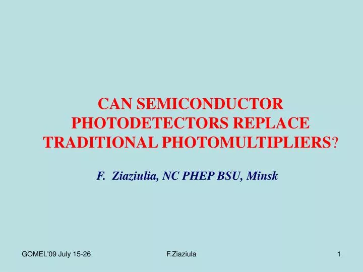
CAN SEMICONDUCTOR PHOTODETECTORS REPLACE TRADITIONAL PHOTOMULTIPLIERS ?. F. Ziaziulia, NC PHEP BSU, Minsk. INTRODUCTION. Photon-counting devices are used for more and more applications, for example in nuclear and high energy physics medicine ecology quantum communication

E N D
CAN SEMICONDUCTOR PHOTODETECTORS REPLACE TRADITIONAL PHOTOMULTIPLIERS? F. Ziaziulia, NC PHEP BSU, Minsk F.Ziaziula
INTRODUCTION Photon-counting devices are used for more and more applications, for example in • nuclear and high energy physics • medicine • ecology • quantum communication • fluorescence spectroscopy • etc, etc. Here the attention will be paid to the first point mainly. For registering the pulse optical low-intensity radiation are used different types of photodetectors - the instruments, which convert photon energy into the electrical signal, the main of them are: • vacuum photomultipliers - PMT, capable of registration separate photons; • semiconductor detectors: -without the internal amplification of charge; -with the internal amplification of charge . F.Ziaziula
THE MAIN PROPERTIES OF PMTBrief introductin. In 1906 Geiger, Marsden and Rutherford scattered alpha-particles on a thin gold foil and determined the scattering angle from the light flash produced at the impact point of the alpha-particles on a phosphor screen .The light detector was the human eye which has a remarkable sensitivity when it is adapted to the dark. In the year 1913 Elster and Geiter invented the photoelectric tube and in 1930 the first photomultiplier tube (PMT) was invented by L. Kubetsky. In 1939 V. Zworykin and his colleagues from the RCA laboratories developed a PMT with electrostatic focusing [3], the basic structure of current PMT’s, and a short time after it became a commercial product. Single photons were detectable from now on. Further innovations have led to highly sophisticated devices available nowadays. PMT’s have two severe handicaps: they are very sensitive to magnetic fields (some devices tolerate axial magnetic fields) and their price is high because the complicated mechanical structure inside a vacuum container is mostly handmade. F.Ziaziula
The main properties of PMT . . F.Ziaziula
Microchannel plate (MCP) F.Ziaziula
Na22 +NaI(Tl) Typical spectrum F.Ziaziula
Block diagrams of high-voltage dividers: (a) resistive, (b) on bipolar transistors, (c) on field-effect transistors, and (d) on composite transistors. Particular rated values of resistors depend on the selected initial current value. The distribution of voltages between the dynodes is given in arbitrary units. F.Ziaziula
Some spectral responses F.Ziaziula
APPLICATION of PMT • UV/Visible/IR Spectrophotometer • Atomic Absorption Spectrophotometer • Photoelectric Emission Spectrophotometer • Fluorescense Spectrophotometer • Raman Spectroscopy • Liquid or gas chromotography • X-ray difractometer • Electron microscopes • Mass Spectroscopy and Solid Surface Analysis • Pollution Monitoring: Dust counter, Turbidimeter, NOx & SOx meters • Biotecnology • Medical Applications: Gamma Camera, Positron CT, In-Vitro Assay, X-ray photometer • Aerospace • Laser : Radar, Fluorescent Lifetime measurement • Plasma • High Energy Physics: Hodoskope, TOF Counter, Cherencov Counter, Calorimeter, Neutrino experiments, Neutrino and Proton Decay Experiments, Neutrino and proton Decay Experiments, Air Shower Counter F.Ziaziula
SMS ECAL Spectrometer ARGUS (IF NANB ) Photodetector of TUS space spectrometer for COSMOS Satellite F.Ziaziula
The crystal ball for the measurement of pibeta decay π+→π0+e++ν followed by π0→γ+γ, which has a branching ratio of 10-8, is made of 240 pure CsI crystals. The crystal readout needs to cover the large area of the rear crystal face, it has to be very sensitive because the light yield of pure CsI is only few percent compared to NaI(Tl) and it has to be fast in order to allow an efficient suppression of accidental coincidences. The choice was a fast 10-stage PMT with 78 mm diameter from Electron Tubes .The PMT’s have a quartz entrance window (emission wavelength of pure CsI is 315 nm) and are directly glued to the crystals. The Muegamma experiment at PSI measure the decay μ+→ e+γ with a sensitivity better than 5⋅1014. The γ’s detected in a 800 l liquid xenon calorimeter by the observation of the scintillation light with 800 PMT’s. The deposited energy derived from the sum of all PMT signals and the position of the γ conversion calculated from the distribution of the individual amplitudes . F.Ziaziula
Super Kamiokande Detector size: 41.4 m (height)X 39.3 m (diameter) {cylinder form}weight : Pure water 50000 toptical sensor: Photomultiplier (a diameter of 50 cm of the largest area in the world) 11200energy precision: 2.5% (for 1GeV) to 16% (for 10MeV)energy threshold: 5MeVplace: Mozumi mine, Kamioka, Japanconstruction cost: about 90 million dollars (10.4 billion yen) (for 6 years 1991-1996) F.Ziaziula
SOLID STATE DETECTORS The main disadvantages, which impede use PMT in some specific applications, are large sizes, the high voltage of power supply and sensitivity to the magnetic fields. Furthermore, during the construction of the systems, which contain hundred thousand channels of registration, important factor becomes the price of detector, which in the case PMT is sufficiently high. These factors became the reason for the active development of the solid-state instruments, which use a phenomenon of the photoconductive effect. The semiconductor detectors of photons can be divided into two large groups: the photodetectors, in which the transformation of light signal occurs • without the internal amplification of charge; • photodetectors with the internal amplification of charge. The first group includes the p-i-n photodiodes, which because of their reliability, compactness and low cost successfully adapt in different physical experiments. The quantum effectiveness of these photodiodes in the maximum of spectral sensitivity reaches 90%. F.Ziaziula
However, with light recording of the short duration (less than 1 μs) it is necessary to use the external wideband amplifier, whose noise does not make it possible to register the flash of light with the number of photons of less than 1000. Furthermore, relatively great thickness of the depletion layer makes p-i-n photodiodes sensitive to others emissions (gamma-quanta, the charged particles). VLSI(Very Large Scale Integration) cheap for the silicon photosensitive co-ordinate detector (“INTEGRAL” PLANT,Minsk). 128 х 128 micropixel (256x256 possible), active readout and contro lwith threshold management. F.Ziaziula
In the detectors of the second group the internal amplification of charge occurs, as a rule, due to the impact ionization of carriers in the high electric fields. Under the action of field free charge carrier (electron or hole) obtain energy, sufficient for the ionization of neutral atom and release one additional electron hole pair, this process can be repeated repeatedly. Semiconductor detectors with the internal strengthening of charge, caused by impact ionization, avalanche photodiodes (APD) ) were developed more than 50 years ago. Merits of APD - high speed operation and quantum effectiveness (to 90%), and also broad dynamic band. Mu-factor of the industrial standards of silica APD, which work in the proportional regime (i.e. with the signal at the output APD, proportional to the intensity of recorded light), comprises ~102 . Thus, to record single photons by the traditional detectors on the basis of p-n junction, which work in the proportional regime of amplification, is impossible. F.Ziaziula
Special technologies make it possible to make APD with the mu-factor to ~103 . With this mu-factor the signal from the single photoelectron can exceed the level of noise of amplifier; however, the fluctuations of multiplication factor in APD do not make it possible to register the light pulses, which contain less than 20-50 photons. To increase the multiplication factor of traditional silica APD to 104 or more is impossible for the thermal breakdown of p-n- junction and the failure of instrument. However the way has been found, allowing to increase amplification. It is a creation of structure in which the avalanche discharge is limited to a feedback mechanism. Works in this direction to Russia were spent at Physical institute of P.N.Lebedev of the Russian Academy of Sciences where the structure of type metal-dielectric-semiconductor (MDS)] was investigated. In such structures carriers appearing during an avalanche collect on border has undressed the semiconductor-dielectric that leads to local decrease in intensity of electric field, reduction of factors of shock ionizationand the termination of formation of an avalanche mode. F.Ziaziula
The basic lacks of MDP-structures - necessity of giving the pulse voltage power supply and degradation of characteristics of the device. Problems have been solved at use of structures metal-resistive a layer-semiconductor (MRS). It has allowed to increase essentially factor of strengthening of a photocurrent (to 104), to improve stability of characteristics, to increase the area of a sensitive surface and service life of devices. Simultaneously in a number of world laboratories possibility of application for registration of single photons of the p-n-junction working in an avalanche mode at voltage above breakdown was studied, i.e. in a Geiger mode Geiger Such detectors named SPAD (Single Photon Avalanche Diode), are capable to register single photons with efficiency to 80 %. In Geiger mode the signal from one photon, arriving on 50 Ohm loading, can make some volt. F.Ziaziula
Lack SPAD - the fixed amplitude output signal and also tolerance of the detector to external influence during the period after operation and till the restoration moment. The next step achieved with the novelphoto-detectors developed in Russia, Silicon Photomultipliers (SiPMs) at the beginning of this millennium. This device can detect single photons like a PMT and therefore some people call it Silicon PhotoMultiplier, SiPM. The pulse height spectrum measured with a G-APD shows a resolution which is even better than what can be achieved with a photomultiplier and even with a hybrid photomultiplier tube. Pulse height spectrum of weak light flashes measured with a G-APD. F.Ziaziula
The MRS (Metal-Resistor-Silicon) structure SiPM (Silicon PhotoMultiplier) is a new type of Geiger-mode avalanche photodiode that shows promise for use with scintillators. They have recently been tested as possible detectors for the hadron calorimeter tiles for the next-generation International Linear Collider. The SiPM is a p-n junction diode that is biased above the breakdown voltage in order to create a Geiger avalanche. SiPM: what is it? Structure of the micropixel of a SiPM. The resulting depletion region in this device is of the order of just 5µm, with an avalanche region of around 1µm. Such a thickness is sufficient for optical photon detection. The Geiger avalanche is passively quenched by a resistive load in series with the diode. In the MRS structure of this SiPM, the resistive load takes the form of a special technology layer deposited on the diode surface. F.Ziaziula
By using the high-resistivity material SiC, the resistor element can be made small whilst providing adequate quenching. A semi-transparent metal contact layer on top of the quenching resistance forms the electrode. SiPM: what is it? F.Ziaziula
SiPMT is a photodetector on the basis of the ordered set (matrix) of the p-n-.junction (cells) executed on the general substrate. The characteristic size of a cell is an order 30-100 microns. Density of packing of a matrix - about 100-1000 cells/mm2. The area of the sensitive surface SiPMT, may lays in limits from 1×1 to 5×5 mm2 and more. All cells are identical. All of them are united in the general point by current-carrying bus. Displacement voltage of all cells the general. It on some volts (value of an overvoltage) exceeds voltage of breakdown of p-n junction. Each cell contains current-limiting resistor. Therefore Geiger breakdown current in a cell is limited. The signal of each cell - logic also does not depend on number of the initial carriers which have caused operation of a cell. SiPMT itself as whole represents the analogue detector as its output signal is equal to the sum of identical signals of the p-n junctions which have operated at absorption by them of photons. F.Ziaziula
The general equivalent circuit of the SiPM. . The photodetection efficiency of SiPM of25(5x5)mm2 with micropixels size of 100x100μm2 (fillingfactor of 64%) at large overvoltages. F.Ziaziula
Microscope picture of a 9(3x3) mm2SiPM. It consists of an array of 5625(7575)micropixelswith 30 x 30 mm2 size. 25(5x 5) mm2 SiPM. It consists of anarray of 1600(4040) micropixels with 100100μm2 size. F.Ziaziula
SiPM 300 pixels F.Ziaziula
The photodetection efficiency of SiPM of 25(5x5) mm2 with micropixels size of 100x100μm2 (filling factor of 64%) at a temperature of-60 C0 is compared with that of a Photomultiplier. F.Ziaziula
The energy resolution of CMS ECAL meets the design goal for the detector. For uniform illumination of a crystal with 120 GeV electrons a resolution of 0.5% was achieved. The avalanche photodiode (APD) developed for the electromagnetic calorimeter of CMS has a thin p-doped layer of silicon in front of the p-n junction where the photo conversion takes place. The created electrons are amplified. The internal gain of an APD improves the signal to noise ratio but the excess noise factor (avalanche fluctuations) and the gain sensitivity to voltage and temperature variations contribute to the energy resolution. • Basic structure of the APD developed for CMS F.Ziaziula
CONCLUSION Solid-state silicon photoelectronic multipliers (SiPMT) - quickly developing class of photodetectors which becomes a basis for the decision of a wide range of the scientific and applied problems demanding registration of pulse radiation of small intensity. Characteristics of modern detectors allow not only to replace vacuum PMT in many applications, but also to create on their basis qualitatively new systems containing thousand of channels of registration: hadron calorimeters, telescopes for gamma astronomy, pozitron tomographs of new generation and so on. Small dimensions, compatibility with standard MOP-TECHNOLOGY and, as consequence, low cost will do this class of photoelectronic devices by a perspective commercial product. Now the stage of laboratory researches of characteristics SiPMT is finished. In the world there was a serious interest to manufacture SiPMT, to their application not only in the accelerating physics, but also in astrophysics, medicine, the industry and so on... F.Ziaziula
The business concerns already letting out first samples of such detectors (Photonique, SensL, RMD) or planning their release (Photonis, Siemens). Company Hamamatsu Photonics developing SiPMT under name MPPC (Multy-Pixel Photon Counter) has achieved the big successes.Already today it is possible to find in the Internet proposal about sale of the detectors similar SiPMT. Their price is still rather high, however it is possible to expect, that in the future it will not exceed several dollars on 1 square мм. F.Ziaziula
MERCI For attention F.Ziaziula
Literature • Кашеваров В.Л., Павлюченко Л.Н, Сокол Г.А. Кремниевые детекторы с внутренним усилением. – Препринт ФИАН, 1994. • Гасанов А.Г., Головин В.М., Садыгов З.Я. и др. — Письма в ЖЭТФ, 1988, т.14, с.706. • Гасанов А.Г., Головин В.М., Садыгов З.Я., Юсипов Ю.Н. — Письма в ЖТФ, 1990, т.16, вып.1, с.14. • Haitz R.H. Model for Electrical Behavior of a Microplasma. – Journal of Applied Physics, May 1964, vol.35, N5, p.1370–1376. • Cova S., Ghioni M., Lacaita A., et al. Avalanche photodiodes and quenching circuits for single-photon detection. – Applied Optics, April 20 1996, v.35, N12. • Bondarenko G., Dolgoshein B., Golovin V. et al. Limited Geiger-mode silicon photodiode with very high gain.– Nuclear Physics B – Proceedings Supplements. Supplement 2, 1998, v.61, p.347–352. • Andreev V. et al. A high-granularity scintillator calorimeter readout with silicon photomultipliers.– NIM A 540, 2005, Issues 2–3, p.368–380. • Sefkow F. Presentation MGPDs for calorimeter and muons sytems: requirements and first experience in the CALICE test beam – http://www-conf.kek.jp/PD07/ • V. M. Grebenyuk, A. I. Kalinin, Nguyen Manh Shat, A.K. Zhanusov, V. A. Bednyakov/ Simulation of the Avalanche Process in the G–APD and Circuitry Analysis of the SiPM. • Farrel R. at al. Nucl. Instr. and Meth. in Phys. Res. A353 (1994) 176–179. • В. А. Калинников, Н. А. Кучинский, В. С. Смирнов, А. Г. Тихонов, Н. В. Хомутов/Mаломощный транзисторный делитель для фотоэлектронных умножителей// ПРИБОРЫ И ТЕХНИКА ЭКСПЕРИМЕНТА, 2006, № 1, с. 1-5 • О.К. БАРАНОВСКИЙ, И.Р. ГУЛАКОВ, А.О. ЗЕНЕВИЧ /Амплитудные характеристики одноквантовых фотоприемников с большой фоточувствительной поверхностью //Доклады БГУИР 2007 июль–сентябрь № 3 (19) P.Buzhan, B.Dolgoshein, L.Filatov et al. Large area silicon photomultipliers:Performance and applications. NIM A, 567 (2006) 76. F.Ziaziula
В. А. Калинников, Н. А. Кучинский, В. С. Смирнов, А. Г. Тихонов, Н. В. Хомутов/Mаломощный транзисторный делитель для фотоэлектронных умножителей//ПРИБОРЫ И ТЕХНИКА ЭКСПЕРИМЕНТА, 2006, № 1, с. 1-5 О.К. БАРАНОВСКИЙ, И.Р. ГУЛАКОВ, А.О. ЗЕНЕВИЧ /Амплитудные характеристики одноквантовых фотоприемников с большой фоточувствительной поверхностью //Доклады БГУИР 2007 июль–сентябрь № 3 (19) P.Buzhan, B.Dolgoshein, L.Filatov et al. Large area silicon photomultipliers:Performance and applications. NIM A, 567 (2006) 76. Z.Sadygov, A.Olshevski, I.Chirikov et al. /Three advanced designs of micro-plxelavalanche photodiodes: their present maximum possibilities and limitatios. //NIM A,567 (2006) 70. M. TESHIMA, B. DOLGOSHEIN, R. MIRZOYAN, J. NINCOVIC, E. POPOVA./SiPM development for Astroparticle Physics applications//arXiv:0709.1808v1 [astro-ph] 12 Sep 2007 V. A. Kalinnikov, N. A. Kuchinskiy, V. S. Smirnov, A. G. Tikhonov N. V. Khomutov and F. E. Zyazyalya/ A Small-Power Transistor Divider for Photomultiplier Tubes/ Dieter Renker /Photodetectors in High Energy Physics//PoS(PD07)001 E. Rutherford, Philosophical Magazine, Series 6, 21 (1911) 669 H. Geiger and E. Marsden, Proceedings of the Royal Society 82A (1909) 495. B.K. Lubsandorzhiev, Nucl. Instr. Meth. A 567 (2006) 236. V.K. Zworykin and J.A. Rajchman, Proc. IRE 27 (1939) 558. P. P. Antich et al., Nucl. Instr. Meth. A 389 (1997) 491. V. Saveliev and V. Golovin, Nucl. Instr. Meth. A 442 (2000) 223. F.Ziaziula
SCINTILLATORS Crystal Properties • YAG:Ce • Yttrium aluminum garnet activated by cerium is fast with excellent mechanical properties and is chemically resistant scintillator. Mechanical properties enable to produce YAG:Ce scintillation screens down to a thickness of 30 µm. YAG:Ce detectors are excellent for electron microscopy, beta and X-ray counting, electron and X-ray imaging screens. • BGO • Bismuth germanate is intrinsic scintillation material with high absorption power. Due to its high effective atomic number and high density, BGO is a very efficient gamma absorber with high photo effect fraction which results in a very good photo peak to Compton ratio. BGO detectors are preferred for medium and high-energy gamma counting and high-energy physics applications. • Nal:Tl • Sodium iodide activated by thallium has long been the scintillation standard. Nal:Tl has good performance, economical price, high luminescence efficiency, very good spectroscopic performance and no significant self absorption of the scintillated light. • YAP:Ce • Yttrium aluminum perovskite activated by cerium is a fast, mechanically strong and chemically resistant scintillation material. Mechanical properties enable precise machining and entrance windows can be made with a very thin aluminum layer deposited directly on the entrance surface of the crystal. YAP:Ce scintillators have very low energy secondary X-ray emissions which makes them desirable for imagining applications. YAP:Ce detectors are used for gamma and X-ray counting, electron microscopy, electron and X-ray imaging screens, and tomography systems F.Ziaziula
CaF:Eu Calcium fluoride activated by Europium is light scintillators are used for detection of charged particles and soft gamma ray up to several hundreds keV. CaF:Eu is typically used for detection of beta rays due to its relatively small back scattering. It is not suitable for detection of high-energy gamma ray because has a small photo fraction. It is non hygroscopic and is relatively chemically inert. CsI:Tl Cesium Iodide activated by thallium is a scintillation material with high absorption power and can be used as an efficient gamma ray absorber. CsI:Tl is soluble in water, but is not hygroscopic in laboratory conditions. It has high resistance to mechanical and thermal shocks. CsI:Tl can be easily fabricated into wide variety of shapes and geometries. It can be also fabricated into detection matrices. LuAG:Ce Lutetium Aluminum Garnet activated by Cerium (chemical formula Lu3Al5O7) is relatively dense and fast scintillation material. Its density of 6.73 g/cm3 is about 94 % of density of BGO (7.13 g/cm3). Decay time is much faster (70 ns) compared to BGO (300 ns). This is advantage for time dependent and coincidence measurements. Wavelength of scintillation emission is about 535 nm, similar as BGO (480 nm), which is ideal for Photodiode and Avalanche Diode readout. This material can by used also for Imaging Screens, similarly to YAG:Ce. The advantage of LuAG:Ce is its higher density allowing for thinner screens with higher spatial resolution. The material is mechanically and chemically stable, it can be machined to variety of shapes and sizes including prisms, spheres, and very thin plates. Its primary advantage high density, fast decay time, a wavelength of luminescence emission well suitable for photodiode and avalanche diode readout, chemical, mechanical, and temperature resistance make it an ideal choice for PET scanners, high energy gamma and charge particle detection, and high spatial resolution Imaging Screens for Gamma, X, Beta and UV ray F.Ziaziula
PWO • Lead tungstate PbWO4 (PWO) is a new "heavy" highly efficient and "fast" scintillator for high energy physics. It has the shortest radiation length and Moliere radius among the known scintillators, satisfactory light yield for this energy range, high radiation stability. Production technology which under continuous development allows to prepare uniform scintillators ensuring high energetic and special resolution of the detecting assembles on accelerators. • NBWO • Double tungstate of sodium and bismuth NaBi(WO4)2 (NBWO) is also a new "heavy", "fast" and optically dense oxide single crystal. Is used as a Cherenkov radiator. • GSO • Gadolinium silicate doped with cerium is a "fast" crystal and can be used as a protection scintillator. Its possible applications include computer tomography, spatial resolution of less than 1 mm. Is the most promising for spectrometry and radiometry of gamma-radiation in the low energy range (<1 MeV). Has good temperature stability, due to which can be used in system equipment. • CWO • Cadmium tungstate CdWO4 (CWO), due to its low intrinsic background and afterglow together with sufficiently high light yield, is the most promising for spectrometry and radiometry of radio nuclides under extremely low activities, and also for computer tomography. Technology of its production is also well developed. • is F.Ziaziula
ZnSe(Te) • ZnSe(Te) single crystals are characterized by the unique combination of high conversion efficiency, intrinsic luminescence in the red region of spectrum, high thermal and radiation stability; they are not hygroscopic, and afterglow is practically absent. Production technology has been developed of "fast" and "slow" scintillation crystals with different decay times and intrinsic luminescence maximum wavelengths. • ZnSe(Te) crystals are not toxic, moisture-resistant, conserve working parameters after gamma-irradiation up to 107 Rad and continuous heating up to 400 K. These qualities make ZnSe(Te) an excellent material for multi-purpose ionizing radiation detectors of the "scintillator-silicon photodiode" type. They are used for radiation monitoring, medical and technical tomography, X-ray medical devices, non-destructive testing systems, customs inspection, spectrometry of alpha- and beta-radiation, as well as soft X-rays. F.Ziaziula
CMS. Fragment of Preshower F.Ziaziula
SPIROC (SiPM Integrated Read-Out Chip): Dedicated very front-end electronics for anILC prototype hadronic calorimeter with SiPM read-out.Technology : AMS 0.8 μm CMOSChip area : ~10mm²Package : QFP-100 F.Ziaziula