Download
1 / 47
470 likes | 590 Views
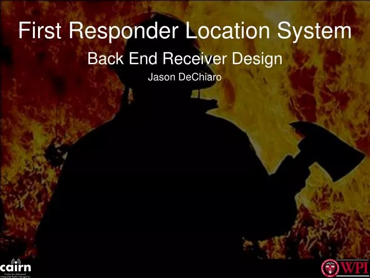
System Overview. Receiver Block Diagram. Back End Block Diagram. Revision Overview. Version 0.0,0.3,0.4 System Targets. BW = 750 Mhz ADC Resolution = 8bits Sampling Rate = 1.5 Gsps Direct RF sampling @ 440Mhz Less complex analog design Less components = less chance of error.

E N D
Version 0.0,0.3,0.4 System Targets • BW = 750 Mhz • ADC Resolution = 8bits • Sampling Rate = 1.5 Gsps • Direct RF sampling @ 440Mhz • Less complex analog design • Less components = less chance of error
ADC Maximum Ratings • 1.5 Gsps Conversion Rate • 2.2 Ghz Full-Power Analog Input Bandwidth • 7.5 Effective Bits at Fin = 750Mhz (Nyquist) • ± 250mV Input Signal Range • Latched, Differential PECL Digital Outputs • Selectable 8:16 Demultiplexer
What Does It All Mean? • At 1.5 Gsps we can do direct RF sampling of a 750Mhz RF signal. • 7.5 Effective Bits = 2.7mV resolution • PECL – ‘Positive Emitter Coupled Logic’ • High speed • Differential • 8:16 Demultiplexer slows the output data rate from 8bits@1.5Ghz to 16bits@750Mhz
Memory Interface Logic Timing Sample 1 Sample 2 Sample 3 Sample 4 Enabled Clock
Recap… • We have 64Bits @ 187.5 Mhz • We need 1.5GB of memory per second of captured data. • Sounds like an SDRAM solution is needed
A bit about SDRAM • Designed for high speed burst reads and writes • Relatively cheap at large capacity • SDRAM used in PC’s is cheap • 1 GB of PC2100 = $109.00
SDRAM Buffer • We need to buffer the bit stream so we can do burst writes • SRAM can be used for this • Also used to allow time for memory refresh
Level conversion • PECL coming from ADC’s • Registers PECL in and out • SRAM TTL or LVTTL
Can We Use 1 FPGA Instead? • Simplify PCB design • Better signal integrity • Chip delavs Vs PCB delays • Ability to change design • Configurable I/O blocks eliminate the need for level conversion
Version 0.1 FPGA Specs • 1 Million gates • 200 Mhz internal clock frequency • 324 general purpose I/O pins – 64 available • $170.00 each (qty 1000)
FPGA Eval Board Components • 32MB SDRAM on board • RS232 capabilities • USB capabilities • 10/100 capabilities
What is a SDRAM controller • Interface between data path and memory • Responsible for: • Data Write Timing • Data Read Timing • Data Refresh • Data Addressing
DDR SDRAM Requirements • Data read/writes occur synchronous to the memory clock • Two data read/write per clock cycle • Memory commands also occur synchronous to the clock • Memory commands ONLY occur on the rising clock edge
Typical DDR SDRAM Timing Diagram Consecutive Write Timing Diagram Data Out Strobe Data Out OutputEnable Micron MT46VXXMXX Data sheet
DDR SDRAM Refresh • Must refresh all rows in any rolling 64mS interval • 64mS/8192Rows (256MB) = 7.8μS average refresh interval • 7.8uS average refresh interval is maintained for higher density DDR SDRAMs JEDEC Standard – JESD79C
DDR SDRAM Buffer • Allows burst writes • Allows streaming input • Allows time for refresh
Where Are We Today • MAX108 ADC • 100 MHZ sampling • 8 bits/sample
Where Are We Today • FPGA running at 200MHZ • 50,000 8-bit Samples stored in FPGA • Drives ADC@100 MHZ • Serial connection to PC at 115,200bps
Where We Are Today • Collect information from FPGA via serial connection • Display Time domain signal
Where We Are Today • Display Frequency domain signal • View sidebands • View carriers
OFDM Signal Captured • Center frequency = 25 MHz • Bandwidth = 10 MHz • Maximum frequency = 30 MHz • Fractional bandwidth = 1/3 • Number of carriers = 8192 • Carrier spacing = 3.6 kHz • Symbol time = 273μS
Current Version 0.1 • Evaluation boards • 50,000 samples • 100 MHz sampling rate • 50 Mhz bandwidth
Ver 0.2 • Evaluation boards • 32 Million samples • 100 MHz sampling rate • 50 MHz bandwidth
Ver 0.3 • Custom PCB • ?? Billion samples • 1.5 Billion samples per second • 750 MHz bandwidth
Layout Issues • Propagation delay • Edge rates (highest freq component) • Trace impedance • Cross-talk • Grounding issues • Power supply issues
Digital Design – Edge rates • Data Ready fall time = 180pS • Most energy contained below = 2.77 Ghz • We need to design for edge rates not bit rates
FPGA DReady output • Rise time = 453.2 pS • Energy contained below 1.1Ghz
FPGA 100MHz Clock Output Differential Probe • Rise time = 1.02 nS • Energy contained below 490Mhz
FPGA 100MHz Clock Output Passive probe • Rise time = 2.9ns • Energy contained below 172.4 Mhz
Review Specifications • 8 bits @ 1.5 Gsps (max) • 1.5 GB/s at max sampling rate • DDR SDRAM memory • High speed PCB design constraints
Typical PECL Input And Output Stage Micrel SY88893V Datasheet