Download
1 / 19
190 likes | 426 Views
ONEBAT Meeting November 17, 2005. EPFL contribution Samuel Rey-Mermet, Paul Muralt. Outline. New design for PEN New photolithographic masks for PEN Process flow CGO dry etching Lift-off Ni plating Patent Main achievements Milestones Future work. New designs for PEN.

E N D
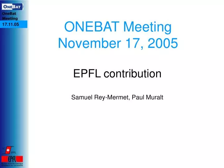
ONEBAT MeetingNovember 17, 2005 EPFL contribution Samuel Rey-Mermet, Paul Muralt
Outline • New design for PEN • New photolithographic masks for PEN • Process flow • CGO dry etching • Lift-off • Ni plating • Patent • Main achievements • Milestones • Future work
New designs for PEN Ni grid without current collector PATENT PENDING Ni grid with current collector
New photolithographic masks 6 Masks: Current collector, electrolyte, seed layer, mould, anode and membrane. Contact anode (4 x 6 mm2) Contact cathode (6 x 4 mm2) Ni grid 2.4 cm Current collector Grid and current collector line width: 5 um Hexagone side: 50 um Hexagone diagonal: 100 um Membrane (diam.5 mm) Connecting lines for eplating
Process Flow Current collector deposition Photo. Mask 1 CC etch Dry etch CC Deposition of electrolyte PATENT PENDING
Process Flow Photo. Mask 2 Electrolyte etch Electrolyte dry etch Photo. Mask 3 Seed layer Deposition seed layer PATENT PENDING
Process Flow Lift-off seed layer Photo. Mask 4 Mould eplating Grid eplating Resist removal PATENT PENDING
Process Flow Depostion porous anode (anode etch ?) Photo. Mask 6 Si etch Si backside etch Depostion porous cathode PATENT PENDING
Process Flow Summary 16 main steps: Wafer 1 is before step 13 Critical points: Lift-off definition Cr/Au must be replaced by Ni Cathode & Anode deposition (LC Ni-CGO ~Ok, NMW) Si dry etch (first test ok) Dicing (Laser?)
CGO dry etching Ar, CF4, CCl4 2.45 GHz ECR Plasma Vbeam Vacc RFchuck Effect of the working pressure and rf power (chuck) on the etching rate of PZT thin film, selectivity for 60 W. RF 13.56 MHz Water cooled
CGO dry etching Etching rate for Vbeam/Vacc=2, at 5 x 10⁻⁴ mBar, with 16 sccm Ar, 2 sccm CCl4, 4 sccm CF4, 80 W RF bias power
Evaporation Designed for lift-off 1.5 10-6 mBar after 1h. Cr, Au, Ti, Al, Ni 1 m
Lift-off Remaining parts of the seed-layer, broken grids… 100 um 100 um Lift-off is improved
Ni eplating Pt CC 100 nm thick Ni grid 5 um thick CGO 150-200 nm thick 100 um
Patent A PCT patent application is being prepared and filed before December 16. Annoying: Patent on grid by semiconductor process (CVD) US 2005/0115889 (Liliput?) filed in 9/2003, 8 months after our invention. Lucky: No conductive grid, no electrolytic deposition claimed
Main achievements Ni grids 100 mm 50 mm Ni grids with CGO
Milestones • WP 1.1 Electrolyte • Dense, crack free, CGO 80/20 OK • Conductivity=0.5 S/m @500°C OK • Microstructure charact. OK • Electrical charac. of membrane not OK • Stress measur. OK • WP 1.2 Anode • Ni-CGO, 500 S/cm @ RT in air, ~OK porosity? • Thermal stability not tested, grid ok • Stress measur. not tested, no problem • WP 1.3 Cathode • LSCF tested by PLD, not OK • Stress not tested, • Stress measur. not tested,
Milestones • WP 1.4 Microfab. and electrical testing • PEN with contacts in progress (anode, cathode from NMW) • 1st PEN in progress (step 12 of 16) • Concept Ni grid OK • Redesign PEN and contact Mask OK, Process Flow in progress • Integration of Ni grid Improvement in progress
Next Fabrication of a PEN including Ni-grid and NMW electrodes wafer 1: status:step #12/16 13=anode dep (NMW), 14/15=Si-etch, 16=cathode dep (NMW) wafers 2-3: with better seed layer lift off and better Ni-grid Thermal stability testing of this 1st PEN. Electrical testing of this 1st PEN.