Download
1 / 2
20 likes | 104 Views
Delay and Peak Power Minimization for On-Chip Buses using Temporal Redundancy. K Najeeb, Vishal Gupta, V. Kamakoti Department of Computer Science & Engineering, IIT Madras, India Madhu Mutyam International Institute of Information Technology, Hyderabad, India. Introduction

E N D
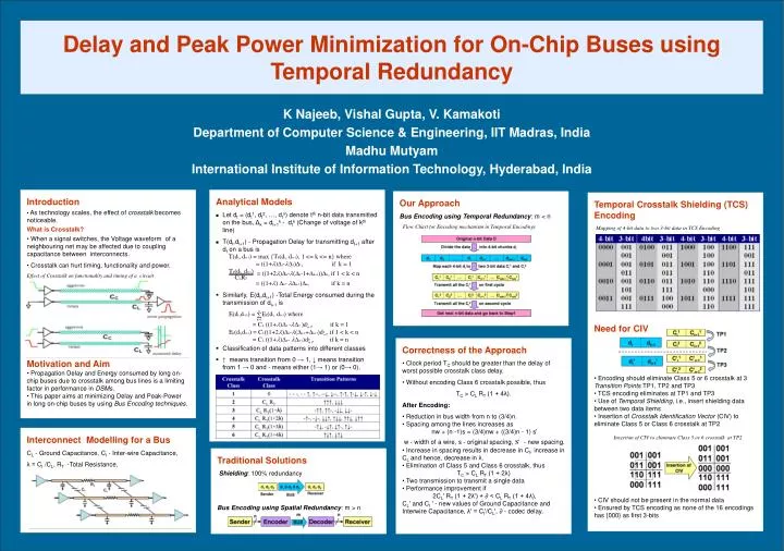
Delay and Peak Power Minimization for On-Chip Buses using Temporal Redundancy K Najeeb, Vishal Gupta, V. Kamakoti Department of Computer Science & Engineering, IIT Madras, India Madhu Mutyam International Institute of Information Technology, Hyderabad, India • Introduction • As technology scales, the effect of crosstalk becomes noticeable. What is Crosstalk? • When a signal switches, the Voltage waveform of a neighbouring net may be affected due to coupling capacitance between interconnects. • Crosstalk can hurt timing, functionality and power. • Effect of Crosstalk on functionality and timing of a circuit • Motivation and Aim • Propagation Delay and Energy consumed by long on-chip buses due to crosstalk among bus lines is a limiting factor in performance in DSMs. • This paper aims at minimizing Delay and Peak-Power in long on-chip buses by using Bus Encoding techniques. • Analytical Models • Let dt = (dt1, dt2, …, dtn) denote tth n-bit data transmitted on the bus, Δk = dt+1k - dtk (Change of voltage of kth line) • T(dt,dt+1) - Propagation Delay for transmitting dt+1 after dt on a bus is • Similarly, E(dt,dt+1) -Total Energy consumed during the transmission of dt+1 is • Classification of data patterns into different classes • ↑ means transition from 0 → 1, ↓ means transition from 1 → 0 and - means either (1→ 1) or (0→ 0). Our Approach Bus Encoding using Temporal Redundancy: m < n • Temporal Crosstalk Shielding (TCS) Encoding • Need for CIV • Encoding should eliminate Class 5 or 6 crosstalk at 3 Transition Points TP1, TP2 and TP3 • TCS encoding eliminates at TP1 and TP3 • Use of Temporal Shielding, i.e., insert shielding data between two data items • Insertion of Crosstalk Identification Vector (CIV) to eliminate Class 5 or Class 6 crosstalk at TP2 • CIV should not be present in the normal data • Ensured by TCS encoding as none of the 16 encodings has {000} as first 3-bits Flow Chart for Encoding mechanism in Temporal Encodings Mapping of 4-bit data to two 3-bit data in TCS Encoding • Correctness of the Approach • Clock period TC should be greater than the delay of worst possible crosstalk class delay. • Without encoding Class 6 crosstalk possible, thus • TC > CL RT (1 + 4λ). • After Encoding: • Reduction in bus width from n to (3/4)n. • Spacing among the lines increases as • nw + (n -1)s = (3/4)nw + ((3/4)n - 1) s' • w - width of a wire, s - original spacing, s' - new spacing. • Increase in spacing results in decrease in CI, increase in CL and hence, decrease in λ. • Elimination of Class 5 and Class 6 crosstalk, thus • TC > CL RT (1 + 2λ) • Two transmission to transmit a single data • Performance improvement if • 2CL' RT (1 + 2λ') + ∂ < CL RT (1 + 4λ), • CL' and CI ' - new values of Ground Capacitance and Interwire Capacitance, λ' = CI'/CL', ∂ - codec delay. Interconnect Modelling for a Bus CL - Ground Capacitance, CI - Inter-wire Capacitance, λ = CI /CL, RT -Total Resistance, Insertion of CIV to eliminate Class 5 or 6 crosstalk at TP2 Traditional Solutions Shielding: 100% redundancy Bus Encoding using Spatial Redundancy: m > n
Data Transmission Mechanism • Crosstalk Class Analyzer (CCA) contains two units • Middle bit Crosstalk Unit (MCU) – checks whether the middle bit of a 3-bit data forms Class 5 or 6 crosstalk with its adjacent bits • Boundary bit Crosstalk Unit (BCU) - checks whether the boundary bit of two 3-bit data items forms Class or 6 crosstalk • Both BCU and MCU work simultaneously to reduce delay • Sender Side • Receiver Side • Experimental Validation • 10mm global bus in top metal layer • Technology parameters from ITRS • Berkeley Predictive Technology Model PTM for calculating capacitance values • D-bit is set if data other than CIV is received • Data is stored for one cycle • D-bit is reset after receiving next data • Decode the stored data and data on the bus to obtain original data Crosstalk Value (CTV) CTV is the measure of number of CIV transmission required. Experimental Results for CTV for different applications • New data is fed to Encoder and CCA simultaneously. It reduces delay. • Encoder encodes the data. • Experimental Results • Use of SimpleScalar 3.0 and SPEC2000 CINT benchmark to simulate performance of buses between processor and L1 I-Cache/D-Cache over 100 million instructions. • Experimental Results for Delay and Peak-Power Reduction on Data and Address Bus • If either of MCU or BCU finds a Class 5 or Class 6 crosstalk, a signal is sent to Encoder, CIV and Latch. • Conclusions • 11% (4%) and 12% (5%) reduction in Address (Data) Bus Delay for 90nm and 65nm Technology respectively. • 46% (24%) and 43% (17%) reduction in Address (Data) Bus Peak Power for 90nm and 65nm Technology respectively. • CIV transmits a zero vector. • Encoder stops sending the encoded data for one cycle. Acknowledgement Supported under BOYCAST fellowship, Department of Science and Technology (DST) India. • If no Class 5 or 6 crosstalk, the sender send the first 3-bits and then the second 3-bits at two cycles. • CIV stops sending a zero vector Synthesis of Encoder and Decoder Design of Encoder, Decoder and Crosstalk Class Analyzer in Verilog and synthesis using Synopsys Design Compiler with 90nm TSMC technology library. Contact Dr. V. Kamakoti Reconfigurable and Intelligent Systems Engineering (RISE) Group Department of Computer Science & Engineering Indian Institute of Technology (IIT) Madras Chennai, TN, India. Ph: (91)-44-22574368 Email: kama@cs.iitm.ernet.in Web: http://vlsi.cs.iitm.ernet.in Power, Delay and Area Overhead of Codec • Decoder maintains a D-bit • Data is discarded if CIV is received