Download
1 / 33
330 likes | 587 Views
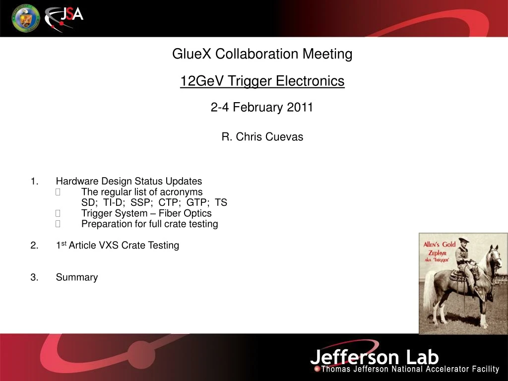
GlueX Collaboration Meeting 12GeV Trigger Electronics 2-4 February 2011 R . Chris Cuevas. Hardware Design Status Updates The regular list of acronyms SD; TI-D; SSP; CTP; GTP; TS Trigger System – Fiber Optics Preparation for full crate testing 1 st Article VXS Crate Testing

E N D
GlueX Collaboration Meeting 12GeV Trigger Electronics 2-4 February 2011 R. Chris Cuevas • Hardware Design Status Updates • The regular list of acronyms • SD; TI-D; SSP; CTP; GTP; TS • Trigger System – Fiber Optics • Preparation for full crate testing • 1st Article VXS Crate Testing • Summary
Trigger Hardware Status • Flash ADC 250Msps ( FADC250 ) • This is where the trigger ‘data’ begins • ** Version 2 design complete – See Fernando’s update ** • Many tests have been completed! • Significant layout revision with consolidation of firmware and FPGA • Crate Trigger Processor ( CTP) • ** 2 units tested in 2009 ** 2 more sent for assembly Sept-2010 • 2 new CTPs assembled and received. New modules have different FPGA and support higher Gigabit speed (5Gbps) • Initial CTP used for verification of new WIENER VXS backplane • New boards will be thoroughly tested and used in full crate test plan • Collects trigger data (SUM) from 16 FADC250 modules within one crate • Transports trigger data over fiber to Global Trigger crate • 10Gbps capability ( 8Gbps successfully tested ) 2
Trigger Hardware Status • Signal Distribution ( SD ) • 2 prototypes tested in 2009 ** Rev-1 ready to manufacturer Oct-2010 ** • Precision low jitter fan-out of ADC clock, trigger and synch signals over VXS backplane to FADC250 modules • Minor revisions to include clock jitter attenuation PLL • 2 Rev-1 boards have been assembled and received • A few power supply issues have been resolved, and updates to firmware have been completed to support jitter attenuation PLLs • I^2C communication with latest TI-D has been tested • We have components for at least six more units • Two boards will be used for full crate testing before ordering pre-production quantities. (June 2011) 3
Trigger Hardware Status • Trigger Interface – Trigger Distribution ( TI - TD ) • FY10 Goals achieved. • FY11 test goals are ahead of schedule and firmware has been completed. • Design changes have been recorded and peripheral modules for TI-D have been completed. (i.e. Fan-out board for CAEN V1290 TDC) • CODA library has been updated for latest TI-D revision. • After full crate testing, pre-production quantities will be ordered. • Direct link to Trigger Supervisor crate • Distributes precision clock, triggers, and sync to crate SD • Manages crate triggers and ReadOut Controller events 4
Trigger Hardware Status • SubSystemProcessor ( SSP ) • Prototype received and is undergoing detailed functional testing!! • FY10 goals achieved and FY11 test activities will continue • Will use SSP during full crate testing in the spring • Collects trigger data from up to 8 front end crates. (2048 channels!) • Trigger data received on front panel with fiber transceivers • 10Gbps input capability ( 4 lanes @3.125Gbps*(8/10b) ) • 10Gpbs output stream to GTP • Global Trigger Processor ( GTP ) (FY10-11) • Schematic work is back on schedule (Scott Kaneta ) • FY11 goal is to build initial prototype and test with SSP and TI-D • Revisions to initial specification has been updated and finalized • Interface requirements to SSP and TS have been finalized • Large scale FPGA has been selected and Xilinx Aurora protocol has been tested with Altera FPGA 5
Trigger Hardware Status • Trigger Supervisor ( TS ) (FY11-12) • New board format – VXS Payload module • Distributes precision clock, triggers, and sync to crate TI-TD • Manages crate triggers and ReadOut Controller events • Direct cable link to Global Trigger Processor (32 trigger bits) • Specification has been updated to match GTP output • Schematic and board layout activities can begin after full DAQ crate testing is complete and pre-production orders for TI-D and other boards have been completed. 6
Ben Raydo Discriminator Status (Not truly trigger system hardware, but very nice new development) • 16 Pre-Production modules have been assembled and received • Significantly cheaper than V895: • -cost < $2,000 • Provides several features not found on V895: • 32bit scalers on all channels at both thresholds • Calibrated pulse widths: from 8 to 40ns • Trimmed input offset (<2mV error) • Second 34pin output connector is fully programmable. • Able to perform logic based on all channels at both thresholds • Final revision has VME64x J1-J2 connector • Full test stand developed by Pedro Toledo(USM – Chile) will be re-used • Hall Groups will test with detectors 16 modules in crate Pre-Production version Note: VME64x connectors 7
Crate Trigger Processor • 4 Fully assembled units are in the lab!! • 2 newest units include VirtexV FX70T that supports higher serial speeds. (5Gbps) Matches FX70T on FADC250 • Initial CTP unit used to verify new WIENER VXS backplane map • Crate Trigger Processor computes a crate-level energy sum (or hit pattern) • Computed crate-level value sent via 10Gbps fiber optics to Global Trigger Crate (32bits every 4ns) CTP Prototype: Board Energy/Hits Up to 10Gbps to CTP Fiber Optics Transceiver VXS Connectors Collect serial data from 16 FADC-250 Crate Sum/Hits 10Gbps Fiber to SSP in global trigger crate 8
N. Nganga 10-Oct-2010 Crate Level – Signal Distribution (SD) -Rev 1 Two boards fully assembled and almost completely tested VITA 41 Switch Slot Connectors 9 14
N. Nganga M. Taylor C. Cuevas Crate Level – Signal Distribution (SD) -Rev 1 • New power regulation scheme tested • New (final) front panel complete • Token In/Out tested • Latest I^2C firmware has been tested with TI-D. • Supports the control of the on board PLLs from • the FPGA via SPI. Users can select Jitter Attenuation mode (PLL) or non-PLL mode. • All common signals from TI ( i.e. Busy, Sync, Trig1, Trig2 have been tested. • Final results from PLL jitter attenuation tests will be completed before 15-Feb-2011 10
Trigger Interface - Distribution W. Gu DAQ Group TID Components VMEPROM (FPGA firmware) Emergency/remote re-programming ‘Legacy’ Trigger Supervisor Interface Xilinx VirtexV LX30T-FG665 VME 64x Eight Optical Transceivers HFBR-7924 VXS P0 TD mode: from SD TI/TS mode: to SD One dedicated link for redundant data collection External I/O (trg, clk…) Trg/Clk/Syc outputs On row_C 11
Trigger Interface - Distribution W. Gu DAQ Group 2/2/2011 • What is tested: • The power distribution for the board is tested and working. • All the discrete components (drivers, buffers, receivers etc) • are tested, and working • The on-board clock distribution network is working. • The on-board trigger distribution network is working. • Serialized trigger data re-sampling (ADN2805). • FPGA firmware: • VME to I2C engine; • VME data readout; • VME remote firmware loading; • Customized the firmware for TI, TD, mini-TS mode • Initial Jitter analysis results for 250MHz clock are low ~2ps 12
TI-TD Testing W. Gu DAQ Group The scope used: Tek7254, probe: TDS3500 differential probe Scope setting: 40GS/sec 25 Ps/Pt, 2.5 GHz limited Measuring software: TDSJIT3 ADVANCED, 400K samples (auto set) or DPOJET ESSENTIAL, 50M samples. Measured on TID#2, TID#1 may be used as clock source TID#1 HFBR #1 TID#2 Mux Clock Osc P0 ClkC ClkA Clock Osc Mux HFBR Buffer HFBR #5 Buffer Measurement diagram DPO7254, TDSJIT3, DPOJET 13
TI-TD Testing W. Gu DAQ Group Assuming that the oscillator has negligible jitters, the TID to P0 distribution has a jitter of less than 2ps, and the two HFBR_7924/34 distribution has a jitter of less than 2ps too ( sqrt(2.65*2.65-1.88*1.88)=1.87ps ). TID#2 on-board oscillator as clock source, the ClkC jitter measured: 1.88ps TID#2, HFBR#5 as clock source, the ClkC jitter measured: 2.65ps 14
Ben Raydo 9-Sept-2010 SSP Prototype Optional DDR2 Memory Module (up to 4GByte) VME64x (2eSST support) VXS-P0 (up to 16Gbps to each GTP) 2x NIM (bidirectional) 4x ECL/PECL/LVDS In 4x LVDS Out 8x Fiber Ports ( 10Gbps each to CTP ) 15
SSP Working with CTP Ben Raydo 9-Sept-2010 SSP CTP 10Gbps ‘Ribbon’ Fiber 4Tx 4Rx 16
SSP 2.5Gbps Fiber Eye (1 of 32 shown) Ben Raydo 9-Sept-2010 FPGA F/O Transceiver Tektronix DSA70000 Fiber optics COAX SSP “Optic Probe” 8GHz Scope Eye analysis 0 Crossing Jitter Time-Interval-Error Single Ended Capture (amplitude is really double what’s seen). Reflections mainly due to test fixture. Very wide receiver eye (0.8UI) at 1E-12 BER. UI = Unit Interval = 1/Bit Rate 400ps Bit Width Gigabit transceivers & optics are performing much better than device specifications – further testing will reveal accurate bit-error rate estimates. 17
SSP Summary Ben Raydo 1-Feb-2011 • BGA assembly issues have been resolved. • SSP will be used for two DAQ crate testing in spring. • Link quality tests remain between fibers and FPGAs, as well as FPGA and FPGA, but is looking very good so far. • DDR2 Memory testing needs to be completed • Testing with GTP will have to wait for GTP prototype. (June ‘11) • SSP Project ahead of schedule! 18
Global Trigger Processor: (GTP) • Global Trigger Processor (GTP) receives all subsystem Level 1 data streams from SSP • Trigger decisions made in GTP and distributed to all crates via the Trigger Distribution (TD) modules in the Trigger Supervisor Crate • Schematics and component selection activities are progressing well • Preliminary component placement and layout strategies have been completed • Xilinx’s ‘Aurora’ Gigabit protocol has been ported to Altera device successfully Trigger Decisions to Trigger Distribution Crate {Trigger Supervisor} 19
Scott Kaneta Jan-2011 Global Trigger - Block Diagram: CTP 1 Global Trigger Crate 4 SSP 1 Payload 1 . . . Trigger Distribution Crate CTP 8 4 / 4 x 8 LVPECL ‘Densishield’ TS GTP Switch A . . . Fiber 32 CTP 121 4 / SSP 16 Payload 16 . . . CTP 128 4 / SD Switch B TI Payload 18 20
Scott Kaneta Jan-2011 Global Trigger Processor: (GTP) Front Panel VXS Backplane Ethernet DDR2 LVDS 36 Transceivers at 8.5 Gbps Ethernet 2 / RGMII RJ45 PHY Altera Stratix IV GX 180 Nios II Processor(s) SSP Data 0 Link Up 0 . . . Code Flash 2 / Multi-Image Configuration Flash Configuration Controller CPLD SSP Data 15 Link Up 15 JTAG Clock, Sync Trig1, Trig2 4 / Fiber Transceiver Legend / 4 High Speed Trigger Out General Purpose 4x Densishield / 32 Configuration 21
Scott Kaneta Jan-2011 Global Trigger Processor: (GTP) VXS Switch Slot Ethernet Altera FPGA JTAG MTP Fiber TxRx / 32 +5VDC 22 LVPECL 4 x 8 pair to TS (P2)
23 Other Trigger System Essentials • VXS and VME64x powered card enclosures • Crate specification complete • Multi-year contract awarded to W-IE-NE-R, Plein & Baus, Ltd. • First article crates (VXS) received 24-Jan-2011 • Acceptance tests nearly complete • (6) –> VME64x & (8) –> VXS crates will be delivered before May-2011 • Will need storage location!! Hartman VXS 21 Slot Backplane CTP @2.5Gbps to each payload port Correctly mapped +5VDC; Ripple Measurement <10mVp-p; 50A load
Other Trigger System Essentials Trigger System Fiber Optics FY11 Work Plan • System diagrams have been updated for Hall D installation 24 • Preparing for procurement now! (Material and installation labor) • Final component specifications are complete • i.e.(Fiber patch panels, Fiber (trunk) cables, MTP patch cables, etc) 23
Two DAQ Crate Testing: FY11 2.5Gbps/ VXS lane Front End Crate: • Several modules have been revised and will need to be thoroughly tested. (FADC250, SD, TI-D) • The initial SSP will be used to sum the trigger data from 2 CTP • Multiple crate ‘system level’ testing is imperative before approving large quantity orders. • Will verify Gigabit serial lanes from each slot • 1st Time for 16 boards!!! • Will measure trigger latency • Will measure trigger rates/VME data rate • Will measure BitErrorRates • Will test using “Playback” mode • (No input cables necessary) • Perfect opportunity to fully test latest revision • of CODA board ‘libraries’ • Plan to use latest CPU as proposed by DAQ group 25
Summary • FY10 board design project goals have been achieved • FY11 plan includes aggressive test plans for all modules • GTP prototype and completion of FINAL revisions for trigger modules in FY11 • High level of detailed design work is exemplary and board tests meet specification • Work activity schedule shows estimate to completion plan is reasonable • Production quantities for all halls have been considered • 2 full DAQ crates with all trigger module units will be tested in spring • Time to think about 4thannual 12GeV Trigger Workshop • Will have plenty of results from full crate testing • Plenty of other work remains for pre-commissioning ‘tools’ and test plans • Weekly 12GeV Trigger meeting continues to produce good discussions and ideas • for implementation of system level test programs and details of hardware designs. 26
Backup Slides All sorts of good stuff
Schedules, work plans for FY11 - FY13 • FY10 design projects are at full resource pace! • FADC250 Latest revision at end of FY10. TEST in FY11. • F1TDC-V2 Work plan moved to FY11 • SD Latest revisions virtually complete. Order, assemble, TEST in FY11 • SSP Prototype received. Initial testing is proceeding nicely. • Further testing in FY11. • TI-TD Prototype(s) received. Initial testing is proceeding nicely. • Firmware development and multi-crate testing in FY11 • 16 Channel LE Discriminator/Scaler (Hall B requirement) • 7 ‘production’ units under test now • VXS Crate Specification Order should be awarded before Oct-10 • GTP Scott Kaneta joins the group! GTP slips to FY11 • TS Specified, and planned for FY11-FY12 • Baseline Improvement Activities (BIA) review on 17-September • FY11 will be an intensive year of significant ‘system’ level testing to assure • that these boards are ready for final production quantity orders in early FY12 20
Level 1 & Trigger Distribution Trigger Decisions Global Trigger Crate Trigger Distribution Crate SSP SSP SSP TD TD TD SSP TD SSP SSP SSP GTP GTP SSP SSP SSP SSP SSP TI TD TD TD TD TD TD TD TD TS SD L1 Subsystem Data Streams (hits & energy) CPU CPU Fiber Optic Links TD can manage 8 TI (Crates) Fiber Optic Links SSP can manage 8 CTP (Crates) Clock Trig1 Trig2 Sync Busy VXS-Crate VXS-Crate Front-End Crates VME Readout to Gigabit Ethernet Up to 128 front-end crates 13
Synchronized Multi-Crate Readout • CTP #2 is also acting as an SSP (by summing the local crate + CTP#1 sum over fiber • A programmable threshold is set in CTP, which creates a trigger when the global sum (6 FADC boards => 96 channels) is over threshold. • Example test with a burst of 3 pulses into 16 channels across 2 crates/6 FADC modules A 2μs global sum window is recorded around the trigger to see how the trigger was formed: Example Raw Event Data for 1 FADC Channel: B. Raydo
2 Crate Energy Sum Testing Global Sum Capture (at “SSP”): Input Signal to 16 FADC250 Channels: Raw Mode Triggered Data (single channel shown only): • Threshold applied to global sum (96 digitized channels) produces 3 triggers. • Raw channel samples extracted from pipeline shown for 1 channel. • Runs at 250kHz in charge mode • Latency: 2.3µs(measured) + 660ns(GTP estimate) < 3µs B. Raydo
Synchronized Multi-Crate Readout Rates • FADC event synchronization has been stable for several billion events @ ~150kHz trigger rate. • Have run up to 140kHz trigger rate in raw window mode, up to 170kHz in Pulse/Time mode. • Ed Jastrzembski has completed the 2eSST VME Interface on FADC allowing ~200MB/s readout Single Crate 12 signals distributed to four FADC250 18% Occupancy B. Raydo