Download
1 / 30
300 likes | 469 Views
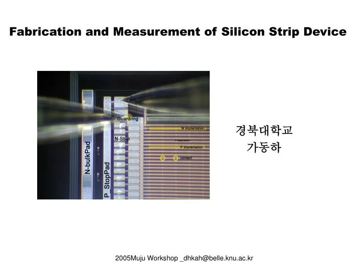
Fabrication and Measurement of Silicon Strip Device. 경북대학교 가동하. Contents. DSSD ( D ouble-side S ilicon S trip D etector) Fabrication Cross-sectional view Processing squence in planar Technology IV & CV TEST – Sensor characteristic curve Measurement method

E N D
Fabrication and Measurement of Silicon Strip Device 경북대학교 가동하 2005Muju Workshop _dhkah@belle.knu.ac.kr
Contents • DSSD (Double-side Silicon Strip Detector) Fabrication • Cross-sectional view • Processing squence in planar Technology • IV & CV TEST – Sensor characteristic curve • Measurement method • Run history and Result view • BEAM TEST – Radiation Hardness • SOURCE TEST – S/N (1 slide) 2005Muju Workshop _dhkah@belle.knu.ac.kr
1. DSSD Fabrication 1. Cross-sectional View N + P + High Resistive n-type substrate Passivation PE-oxide(9,000Å) ILD LTO (앞면:5500Å, 뒷면:4000Å) Initial Oxide(~4,500Å) P + IMD PE-oxide(40,000Å) 2005Muju Workshop _dhkah@belle.knu.ac.kr
1. DSSD Fabrication 2. Process Sequence Process Desc. Remark. No Process Flow & Cross section 1. 2. 3. 4. 5. 6. Start Material ; n-type, (100), 5K .cm. 380m, Front & Back Polished Cleaning ; STD1 Thermal Oxidation; 900C, H2/O2, 6500Å P+ Photo;Mask #F1, <Front> Positive PR, C-Aligner Oxide RIE ; 5500Å PR Strip 7. 8. 9. 10. 11. 12. 13. P+ Photo;Mask #B1, <Back> Positive PR, C-Aligner Oxide RIE & Wet Etch; 5500Å /1000Å+30% PR Strip Cleaning ; STD1 Oxidation; 850C, H2/O2, 200Å P+ implant; B11, 3E15, 40KeV < Front & Back > Oxide Wet Etch; 2000Å 2005Muju Workshop _dhkah@belle.knu.ac.kr
1. DSSD Fabrication 2. Process Sequence (계속) Process Desc. Process Flow & Cross section Remark. No 14. 15. 16. 17. 18. 19. 20. Cleaning ; STD1 Anneal ; 900C, N2, 30min Oxidation; 900C, H2/O2, 1000Å N+ Photo;Mask #F2, <Front> Positive PR, C-Aligner Oxide RIE & Wet Etch; 4000Å / 1000Å+30% N+ implant ; P11, 3E15, 50KeV PR Strip 15. Oxidation 필요여부 21. 22. 23. 24. 25. 26. 27. 28. Cleaning ; STD1 Oxidation & drive in; 900C,H2/O2, 500Å / N2, 170min LTO Oxide Depo.; <Front & Back>6000Å Cleaning ; STD1 LTO Annealing ; 900℃, 30min Contact Photo; Mask #F3, <Front> Positive PR, C-Aligner Oxide RIE & Wet Etch; 5500Å / 1500Å+30% PR Strip • LTO 도포시 양면 도포를 • 위한 Loading • * 23, 24 Step Skip 고려 2005Muju Workshop _dhkah@belle.knu.ac.kr
1. DSSD Fabrication 2. Process Sequence (계속) Process Spec. Process Flow & Cross section Remark. No 29. 30. 31. 32. 33. 34. Cleaning 50:1 BHF,300sec Metal1 Deposition;<Front> TiW/Al1%Si/TiW =1000/10000/750A Metal1 Photo;Mask #F4, <Front> Positive PR, C-Aligner Metal1 Etch; PR Strip PECVD Oxide Depo. ;<Front> 20,000Å * 수회 나누어서 진행 35. 36. 37. 38. 39. 40. 41. 42. 43. Contact Photo; Mask #B2, <Back>Positive PR, C-Aligner Oxide RIE & Wet Etch; 3000Å / 1000Å+30% PR Strip Cleaning 50:1 BHF,300sec Metal1 Deposition;<Back>TiW/Al1%Si/TiW =1000/10000/4000A Metal1 Photo;Mask #B3, <Back>Positive PR, C-Aligner Metal1 Etch; PR Strip PECVD Oxide Depo. ;<Back>40,000Å * 수회 나누어서 진행 2005Muju Workshop _dhkah@belle.knu.ac.kr
1. DSSD Fabrication 2. Process Sequence (계속) Process Spec. Process Flow & Cross section Remark. No 44. 45. 46. 47. 48. 49. 50. 51. 52. 53. Via Photo;Mask #B4, <Back>Positive PR, C-Aligner Oxide Wet Etch & RIE ; 7500Å / 33,000Å+30% PR Strip DI Rinse & NMD-3(Polymer제거 ) DI Rinse & Dehydrate Metal2 Deposition;<Back>TiW/Al1%Si/TiW =1000/10000/750A Metal2 Photo;Mask #B5, <Back> Metal2 Etch PR Strip PE-Oxide Depo;<Back>,8000A * 수회 나누어서 진행 54. 55. 56. 57. 58. 59. 60. 61. 62. PAD Photo;Mask #B6, <Back> PAD Oxide Etch;8000A +30% PAD TiW Etch;750A +30% PR Strip PAD Photo;Mask #F5, <Front> PAD Oxide Etch ;9000A +30% PAD TiW Etch;750A+30% PR Strip H2 Annealing;420C, H2/N2 2005Muju Workshop _dhkah@belle.knu.ac.kr
2. Sensor Characteristic Curve – IV & CV TEST 2.1 Measurement method 2.2 Sensor Fabrication History and Result View 2005Muju Workshop _dhkah@belle.knu.ac.kr
2. Sensor Characteristic Curve 2.1.1 Sensor Mesurement Method – N side TEST (Surface Character) P-STOP_pad -HV N_side_pad +HV P -HV+ I N 2005Muju Workshop _dhkah@belle.knu.ac.kr
p+ guard-ring pad Silver paste N-side p+ strip pad n bulk pad p-guardring p-strip 14 um 380 um 10 um 6 um 30 um 95 um p-stop n-strip n-guardring n-bulk for test 2. Sensor Characteristic Curve 2.1.2 Sensor Mesurement Method – P side TEST (Bulk Character) +High voltage GND 2005Muju Workshop _dhkah@belle.knu.ac.kr
200 2.2 Sensor Fabrication History 1. 1차 Run 공정 History (C-sensor) (a). P-strip Guardring Current • Initial Oxidation 6500A • FPSD Dry Etch 5500A • BPSD Dry Etch 5500A • Wet Etch 1000A + 50% • Buffer Oxidation 200A • PSD Implant B11, 40K, 3E15 (양면) • Anneal, 900C, 30min • Block Oxidation 1000A • FNSD Dry + Wet Etch • NSD Implant P31, 50K, 3E15 (앞면) • Anneal, 900C, 100min • LTO Dep. & Densification(900C, 30min) (b). N-strip Guardring Current • P-strip Fail : 多 • P-strip Leakage ~ 1nA/strip @100V • P-guardring Current ~ 1mA @ 100V N-strip Current (1st Sweep) • N-strip Leakage ~ 0.2nA/strip @30V • N-guardring Current ~ 500nA @30V N-strip Current (2nd Sweep) 2005Muju Workshop _dhkah@belle.knu.ac.kr
2.2 Sensor Fabrication History 2. 2차 Run 공정 History (D-sensor) (a). P-strip Guardring Current • Initial Oxidation 6500A • FPSD Dry Etch 5500A • BPSD Dry Etch 5500A • Wet Etch 1000A + 50% • Buffer Oxidation 200A • PSD Implant B11, 40K, 3E15 (양면) • Anneal, 900C, 30min • Block Oxidation 1000A • FNSD Dry + Wet Etch • NSD Implant P31, 50K, 5E15 (앞면) • Anneal, 1000C, 100min • LTO Dep. & Densification(900C, 30min) Fail Strip (b). N-strip Guardring Current • P-strip Fail : 多 • P-strip Leakage ~ 6nA/strip @100V • P-guardring Current ~ 200uA @ 100V • * Fail Strip이 없는 Sample도 있음 • N-strip Leakage ~ 0.5nA/strip @30V • N-guardring Current ~ 2uA @30V 2005Muju Workshop _dhkah@belle.knu.ac.kr
2.2 Sensor Fabrication History 3. 3차 Run 공정 History (E-sensor) (a). P-strip • Initial Oxidation 400A • LPCVD Nitride 4000A • FNSD Dry Etch Nitride 4000A • NSD Implant P31, 50K, 5E15 (앞면) • FPSD Dry Etch Nitride 4000A • FPSD Implant B11, 40K, 3E15 (앞면) • BPSD Dry Etch Nitride 4000A • Wet Etch Oxide 400A • Buffer Oxidation 200A • BPSD Implant B11, 40K, 3E15 (뒷면) • Anneal, 900C, 120min • LTO Dep. & Densification(900C, 30min) (b). N-strip • P-strip Fail : 없음 • P-strip Leakage : 8 ~ 50nA/strip @100V • P-guardring Current ~ 1uA @ 100V • * 4매(12 Chip 중) 3매(9 Chip) Fail Strip 無 • * Nitride 대신 TEOS의 경우 Fail Strip 多 • N-strip Leakage : 2 ~ 20nA/strip @30V • N-guardring Current ~ 1uA @ 30V 2005Muju Workshop _dhkah@belle.knu.ac.kr
2.2 Sensor Fabrication History 4. 4차 Run 공정 History (G-sensor) • Initial Oxidation 6500A • LP-Nitride 1600A • FPSD Dry Etch 1600A/5000 A • BPSD Dry Etch 1600A/5000 A • Wet Etch 1500A+50% • Buffer Oxidation 400A • PSD Implant B11, 40K, 3E15 (양면) • LP-Nitride 1000A • FNSD Dry+Wet Etch 2600A/5000A/1500A • Buffer Oxidation 300A • FNSD Implant P31, 50K, 5E15 • Nitride Strip • Anneal, 900C, 140min • LTO Dep. & Densification(900C, 30min) • P-strip Fail : 多 • P-strip Leakage : 7 ~ 80nA/strip @100V • P-guardring Current 0.5 ~ 1200 uA @ 100V • * 6매(18 Chip) 중 2매(3 Chip) Fail Strip 無 2005Muju Workshop _dhkah@belle.knu.ac.kr
2.2 Sensor Fabrication History 5. TEST Run 공정 History (a). #01, 02_Oxide Only(작은 그림은 양호한 Chip) Guardring Current • Initial Oxidation 9000A (#01, #02) • Initial Oxidation 9000A + LP-Nitride 4000A • (#03~06) • FNSD Dry Etch + Wet Etch • Oxidation 300A • FNSD Implant P31, 50K, 5E15 • FPSD Dry Etch + Wet Etch • FPSD Implant B11, 40K, 3E15 • BPSD Dry Etch + Wet Etch • Oxidation 300A • BPSD Implant B11, 40K, 3E15 • Anneal, 900C, 140min (#01~04) • Anneal, 900C, 70min (#05~06) • LTO Dep. & Densification(900C, 30min) Fail Strip (b). #04~06 (Oxide +Nitride) • Oxide Only • - P-strip Fail : 多 • - P-strip Leakage : 3 ~ 10nA/strip @100V • Oxide + Nitride • - P-strip Leakage Variation 大 • - N-strip to P-stop Short 2005Muju Workshop _dhkah@belle.knu.ac.kr
CV curve (Capacitor – Voltage) 2005Muju Workshop _dhkah@belle.knu.ac.kr
3.BEAM TEST - Radiation Damage Test 원자력병원 양성자 가속기(35Mev) DSSD sensor 8개, CREAM sensor 3개 (Calibration test sensor 1개씩포함)-총11개 센서사용 1011 ,1012 ,1013 ,1014 ,1015 [양성자갯수/cm2 ] 2005Muju Workshop _dhkah@belle.knu.ac.kr
Sensor Monitor Al Window (2mm) colliminator 직경1cm A2 35 Mev 26 Mev DSSD A1 3.1 BEAM TEST Log table and test Schematic 1.Log table Number of Proton[갯수/cm2] = Target Proton X 80% 2.Test Schematic 2005Muju Workshop _dhkah@belle.knu.ac.kr
3.2.Beam Test Result View - IV curve 2005Muju Workshop _dhkah@belle.knu.ac.kr
4.Sensor Source Test (DSSD E3T1) No Source Noise Test Beta Source Signal Test 2005Muju Workshop _dhkah@belle.knu.ac.kr
SUMMARY and Plan • 1st Design Sensor - 1st,2nd,3rd ,4th Run done • New Fabrication(2nd Design) is just started • a lot takes 3 months • Beam Test • Calculate Damage parameter • Measure Annealing Sensor • Source Test • Complete DAQ System , S/N • X-ray source Image Test • Making Hybrid Board Prototype • Sensor(DC-type) + RC chip + VA Chip END - Thanks 2005Muju Workshop _dhkah@belle.knu.ac.kr
Back up Slide 2005Muju Workshop _dhkah@belle.knu.ac.kr
Pside_IV_measurement _ HV + P P 전도성고무 P P N N N N N Probe Tip P A Wafer E-field _ HV + P 전도성고무 _ HV + Chuck Reverse Bias N 2. Sensor Characteristic Curve 2.2. Sensor Mesurement Method – P side TEST (Bulk Character) <사진>전도성고무 구멍은 Chuck과 Wafer 를 진공으로 고정시키기위해… 2005Muju Workshop _dhkah@belle.knu.ac.kr
K사 6517 HV source P P P P N N N N N P HP 4277A LCZ meter 2. Sensor Characteristic Curve 3.IV&CV Measurement Device Clearning Room IV CV 2005Muju Workshop _dhkah@belle.knu.ac.kr
Sensor Faraday Cup Al Window (2mm) 35 Mev 26 Mev Calibration 1 nA 1X10⁻⁹ X [갯수 X 전하/초] X [초/전하] = [양성자 갯수] 1X10⁻⁹ X [초/1.6X10-9 C] = 1/1.6 X 1010 [갯수] 계획 irradiation 테스트 1011~1015 [양성자갯수/cm2] 2005Muju Workshop _dhkah@belle.knu.ac.kr
Sensor Faraday Cup Al Window (2mm) colliminator 직경1cm A2 35 Mev 26 Mev G5T1 A1 Calibration Input Beam Current 와 Faraday Cup output 비교 A1 ,A2 Current Meter 센서에 원하는 양의 양성자 갯수를 조사하기 위해서 A1과 A2 의 비율 조사 2005Muju Workshop _dhkah@belle.knu.ac.kr
Beam Test Log table Number of Proton[갯수/cm2] = Target Proton X 80% 2005Muju Workshop _dhkah@belle.knu.ac.kr
TH900 evt10000 No Source TH1000 evt10000 Source Test 2005Muju Workshop _dhkah@belle.knu.ac.kr
CV curve (Capacitor – Voltage) 2005Muju Workshop _dhkah@belle.knu.ac.kr
Schematics of Readout and DAQ for DSSD RC chip Wire bonding DSSD HV VA1(-TA) Control Signal FPGA USB2DAQ FADC 2005Muju Workshop _dhkah@belle.knu.ac.kr