Download
1 / 18
220 likes | 450 Views
Radiation Effects on Emerging Electronic Materials and Devices. Ron Schrimpf Vanderbilt University Electrical Engineering & Computer Science Department Institute for Space and Defense Electronics. Radiation Effects in Emerging Electronic Materials and Devices. Approach. Motivation.

E N D
Radiation Effects on Emerging Electronic Materials and Devices Ron Schrimpf Vanderbilt University Electrical Engineering & Computer Science Department Institute for Space and Defense Electronics
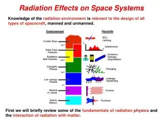
Radiation Effects in Emerging Electronic Materials and Devices Approach Motivation • Experimental analysis of state-of-the-art technologies through partnerships with semiconductor manufacturers • Identification of critical mechanisms through first-principles modeling • Implementation and application of a revolutionary multi-scale radiation-effects simulation tool to identify key challenges and develop hardening approaches • More changes in IC technology and materials in past five years than previous forty years—impact on radiation response is dramatic Impact Selected Results • Design tools and methods demonstrated for future rad-hard technologies • Greatly improved error-rate analysis tools allow implementation of more reliable space electronics • First radiation-effects characterization of most advanced technologies (strained Si, HfSiON, etc.)—essential for deployment of state-of-the-art electronics in DoD systems • Development of most accurate rate-prediction tool to date • Identification of tungsten as key rad-effects issue • Fabrication of rad-hard, reliable alternative gate dielectrics • Demonstration of extremely rad-hard SiGe technology • First examination of rad effects in strained-Si CMOS
Vanderbilt Radiation Effects Program World’s largest university-based radiation effects program • 10 faculty with decades of rad-effects experience • 30 graduate students • A few undergraduate students • Open access • Hundreds of technical publications • Basic research and support of ISDE engineering tasks • Training ground for rad-effects engineers Radiation Effects Research (RER) Group Institute for Space and Defense Electronics (ISDE) • 15 full time engineers • 2 support staff • Limited access, ITAR compliant, IP protection • Document control, milestone tracking, structured management • Task driven support of specific radiation effects engineering needs in government and industry • Faculty fellows with extensive expertise in radiation-effects • Vanderbilt Beowulf supercomputing cluster and ISDE mini cluster • Custom software codes • EDA tools from multiple commercial vendors • Multi-million $ aggregate annual funding • Test and characterization capabilities and partnerships
Team Members • Vanderbilt University • Electrical Engineering: Mike Alles, Dan Fleetwood, Ken Galloway, Marcus Mendenhall, Lloyd Massengill, Robert Reed, Ron Schrimpf, Bob Weller • Physics: Len Feldman, Sok Pantelides • Arizona State University • Electrical Engineering: Hugh Barnaby • University of Florida • Electrical and Computer Engineering: Mark Law, Scott Thompson • Georgia Tech • Electrical and Computer Engineering: John Cressler • North Carolina State University • Physics: Gerry Lucovsky • Rutgers University • Chemistry: Eric Garfunkel, Len Feldman, Gennadi Bersuker
Schedule—May 25 AM 0825 Welcome (Kitt Reinhardt) 0830 MURI Overview (Ron Schrimpf, Vanderbilt University) 0850 Overview: Atomic-Scale Theory of Radiation-Induced Phenomena (Sokrates Pantelides, Vanderbilt University) 0920 Effect of Ambient Hydrogen on Radiation-Induced Interface-Trap Formation (David Hughart, Vanderbilt University) 0940 Overview: Radiation Effects in Emerging Materials (Len Feldman, Vanderbilt University and Rutgers University) 1000 Break 1030 Radiation Effects in Advanced Gate Stacks (Eric Garfunkel, Rutgers University & Gennadi Bersuker, Sematech) 1050 Total Dose Effects in in SiC and Ge MOS Devices (Cher Zhang, Vanderbilt University) 1110 Defects in Non-Crystalline and Nano-Crystalline Alternative Transition Metal Dielectrics (Gerry Lucovsky, North Carolina State University)
Schedule—May 25 PM 1300 Radiation Effects in SiGe Devices (John Cressler and Stan Phillips, GT) 1340 Total Ionizing Dose and Single Event Effects in Strained Si Technologies (Scott Thompson and Hyunwoo Park, University of Florida) 1400 Physics for Simulation of Single Event Transients (Dan Cummings and Mark Law, University of Florida) 1420 Applications of Monte Carlo Radiative Energy Deposition (MRED) to Advanced Technologies (Robert Reed and Bob Weller, Vanderbilt University) 1440 Break 1510 Single-Event Transient Pulse-Width Measurements in Advanced Technologies (Matt Gadlage, Vanderbilt University) 1530 Modeling Total Ionizing Dose Effects in Deep Submicron Bulk CMOS Technologies (Hugh Barnaby, Arizona State University) 1550 Layout-related stress effects on TID-induced leakage current (Nadia Rezzak and Mike Alles, Vanderbilt University) 1610 Total-Dose Effects on MSDRAMs (Farah El-Mamouni, Vanderbilt University) 1630 Radiation Effects on ZRAMs (Enxia Zhang, Vanderbilt University)
Eleven years ago… • Semiconductor technology changing rapidly • Little knowledge of impact on radiation response • Relatively little basic research on radiation effects in emerging technologies
Today • MURI is coming to a close • What was the impact? • Was it basic research? • Was it successful? • What’s next?
A few metrics… • Personnel (2008-09) • 18 graduate students • 3 post-docs • 10 professors • Publications • More than 70 appeared in print in 2008-09
NSREC Basic Mechanisms • 2010: 5/8 papers • 2009: 5/8 papers • 2008: 6/11 papers • 2007: 7/12 papers • 2006: 7/13 papers
Previous MURI • 2005: 6/9 papers • 2004: 8/17 papers • 2003: 5/12 papers • 2002: 7/16 papers • 2001: 5/13 papers • 2000: 7/17 papers
What next for rad effects? • New materials • Carbon-based electronics (i.e., CNTs, graphene, SiC, and diamond), GaN, and antimonide-based semiconductors • High-k dielectrics • Hf-based dielectrics • Si and compound-semiconductor substrates • Alternate-channel devices on Si • Graphene • Compound-semiconductor channels on Si
What next for rad effects? • Small-device phenomena • Device-to-device interactions • Upsets that require charge collection at multiple nodes • single-particle displacement effects • Emerging-device effects • Charge collection in graphene-based devices, carbon nanotubes, and FinFETs • Total-dose and single-event effects in emerging power devices, particularly those based on GaN and SiC
What next for rad effects? • Mechanisms of charge generation and transport • Energy deposition in nanoscale volumes • Surface effects • Transport and recombination at very short times • Transport and recombination at very high carrier concentrations and gradients • Transport and recombination in heterostructures
What next for rad effects? • Si CMOS? Effects mentioned previously, plus… • Very small geometries (<20 nm) • All events affect multiple nodes/devices/circuits • Incorporation of other technologies on Si • Overlayer effects • Ultralow-power effects • Multi-scale, hierarchical analysis • New architectures
Radiation Effects in Emerging Electronic Materials and Devices:Results Radiation Response of New Materials Impact of New Device Structures • Incorporation of new materials dramatically impacts radiation response • HfO2-based dielectrics and emerging high-k materials tested; HfSiON and Ge substrates very promising • Substrate engineering (strained Si, Si orientations, Si/SiGe, SOI) offers possibility for single-event hardening • New device technologies strongly impact single-event response and TID leakage current • SiGe HBTs, strained Si CMOS, ultra-small bulk CMOS exhibit complicated charge collection mechanisms • Strain can improve the TID response of scaled CMOS technologies Localized Radiation Damage Single Events in New Technologies • New rate prediction approach based on combined experiments and Monte Carlo simulation • Passivation/metallization found to dominate SEE response in some hardened technologies • Excellent agreement with on-orbit data; conventional rate-prediction methods underestimate rate by orders of magnitude • Evidence of particle-induced micro-melting in small devices • First physically-based explanation of single-event dielectric rupture • Temporary conducting paths formed in dielectrics by energetic particles
Collaborations • Government: DTRA, NASA, Navy, Sandia, Oak Ridge National Lab • Industry: IBM, Intel, Texas Instruments, Freescale, Jazz, National Semiconductor, Lockheed-Martin, CFDRC, SRC/Sematech, Accelicon • University: IMEC, INPG (Grenoble), Griffith University, MIT/LL