Download
1 / 84
840 likes | 846 Views
ECE 545 Lecture 11. Modern FPGA D evices ATHENa - Automated Tool for Hardware EvaluatioN. Required Reading. Xilinx, Inc. Virtex-5 FPGA Family Virtex-5 FPGA User Guide Chapter 5: Configurable Logic Blocks (CLBs). Required Reading. Altera, Inc. Stratix III FPGA Family

E N D
ECE 545 Lecture 11 Modern FPGA DevicesATHENa - Automated Tool for Hardware EvaluatioN
Required Reading Xilinx, Inc. Virtex-5 FPGA Family Virtex-5 FPGA User Guide Chapter 5: Configurable Logic Blocks (CLBs)
Required Reading Altera, Inc. Stratix III FPGA Family Stratix III Device Handbook 1. Stratix III Device Family Overview 2. Logic Array Blocks and Adaptive Logic Modules in Stratix III Devices
High-Performance Xilinx FPGAs ECE 448 – FPGA and ASIC Design with VHDL
Virtex 5 Arrangement of Slices within the CLB
Row and Column Relationship between CLBs and Slices
Major Differences between Xilinx Families Spartan 3 Virtex 4 Virtex 5, Virtex 6, Spartan 6 Look-Up Tables 4-input 6-input Number of CLB slices per CLB 4 2 Number of LUTs per CLB slice 2 4
64 x 1 Quad Port
64 x 3 Simple Dual Port
Fast Carry Logic Path
Major Differences between Xilinx Families Spartan 3 Virtex 4 Virtex 5, Virtex 6, Spartan 6 Maximum Single-Port Memory Size per LUT 16 x 1 64 x 1 Maximum Shift Register Size per LUT 16 bits 32 bits Number of adder stages per CLB slice 2 4
Low-cost Altera FPGAs ECE 448 – FPGA and ASIC Design with VHDL
Altera Cyclone III Logic Element (LE) – Normal Mode
Altera Cyclone III Logic Element (LE) – Arithmetic Mode
High-Performance Altera FPGAs ECE 448 – FPGA and ASIC Design with VHDL
Altera Stratix III Adaptive Logic Modules (ALM) – Normal Mode
Template for Seven-Input Functions Supported in Extended LUT Mode
Altera Stratix III, Stratix IV Adaptive Logic Modules (ALM) – Arithmetic Mode
Performing Operation R = (X < Y) ? Y : X
Three Operand Addition Utilizing Shared Arithmetic Mode
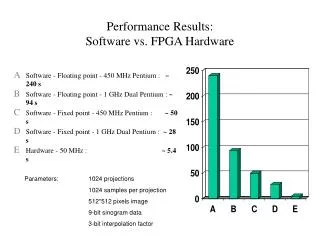
Example of Resource Utilization Report (1) +--------------------------------------------------------------------------+ ; Fitter Resource Usage Summary ; +-------------------------------------------------+------------------------+ ; Resource ; Usage ; +-------------------------------------------------+------------------------+ ; ALUTs Used ; 415 / 38,000 ( 1 % ) ; ; -- Combinational ALUTs ; 415 / 38,000 ( 1 % ) ; ; -- Memory ALUTs ; 0 / 19,000 ( 0 % ) ; ; -- LUT_REGs ; 0 / 38,000 ( 0 % ) ; ; Dedicated logic registers ; 136 / 38,000 ( < 1 % ) ; ; ; ; ; Combinational ALUT usage by number of inputs ; ; ; -- 7 input functions ; 0 ; ; -- 6 input functions ; 287 ; ; -- 5 input functions ; 0 ; ; -- 4 input functions ; 24 ; ; -- <=3 input functions ; 104 ; ; ; ; ; Combinational ALUTs by mode ; ; ; -- normal mode ; 335 ; ; -- extended LUT mode ; 0 ; ; -- arithmetic mode ; 80 ; ; -- shared arithmetic mode ; 0 ;
Example of Resource Utilization Report (2) ; Logic utilization ; 701 / 38,000 ( 2 % ) ; ; -- Difficulty Clustering Design ; Low ; ; -- Combinational ALUT/register pairs used in final Placement ; 476 ; ; -- Combinational with no register ; 340 ; ; -- Register only ; 61 ; ; -- Combinational with a register ; 75 ; ; -- Estimated pairs recoverable by pairing ALUTs and registers as design grows ; -54 ; ; -- Estimated Combinational ALUT/register pairs unavailable ; 279 ; ; -- Unavailable due to Memory LAB use ; 0 ; ; -- Unavailable due to unpartnered 7 LUTs ; 0 ; ; -- Unavailable due to unpartnered 6 LUTs ; 279 ; ; -- Unavailable due to unpartnered 5 LUTs ; 0 ; ; -- Unavailable due to LAB-wide signal conflicts ; 0 ; ; -- Unavailable due to LAB input limits ; 0 ;
Example of Resource Utilization Report (3) ; Total registers* ; 136 ; ; -- Dedicated logic registers ; 136 / 38,000 ( < 1 % ) ; ; -- I/O registers ; 0 / 2,752 ( 0 % ) ; ; -- LUT_REGs ; 0 ; ; ALMs: partially or completely used ; 360 / 19,000 ( 2 % ) ; ; Total LABs: partially or completely used ; 42 / 1,900 ( 2 % ) ; ; -- Logic LABs ; 42 / 42 ( 100 % ) ; ; -- Memory LABs ; 0 / 42 ( 0 % ) ; ; ; ; ; User inserted logic elements ; 0 ; ; Virtual pins ; 0 ; ; I/O pins ; 20 / 488 ( 4 % ) ; ; -- Clock pins ; 5 / 16 ( 31 % ) ; ; -- Dedicated input pins ; 0 / 12 ( 0 % ) ; ; Global signals ; 2 ; ; M9K blocks ; 0 / 108 ( 0 % ) ; ; M144K blocks ; 0 / 6 ( 0 % ) ; ; Total MLAB memory bits ; 0 ; ; Total block memory bits ; 0 / 1,880,064 ( 0 % ) ; ; Total block memory implementation bits ; 0 / 1,880,064 ( 0 % ) ; ; DSP block 18-bit elements ; 0 / 216 ( 0 % ) ; ; PLLs ; 0 / 4 ( 0 % ) ; ; Global clocks ; 2 / 16 ( 13 % ) ;
Resources • ATHENa website • http://cryptography.gmu.edu/athena
ATHENa – Automated Tool for Hardware EvaluatioN Supported in part by the National Institute of Standards & Technology (NIST)
ATHENa Team John MS CpEstudent Venkata “Vinny” MS CpEstudent Ekawat “Ice”PhD CpEstudent Marcin PhD ECEstudent Michal PhD exchange student from Slovakia Rajesh PhD ECEstudent
http://cryptography.gmu.edu/athena ATHENa – Automated Tool for Hardware EvaluatioN • Benchmarking open-source tool, • written in Perl, aimed at an AUTOMATED generation of • OPTIMIZED results for • MULTIPLE hardware platforms Currently under development at George Mason University.
Why Athena? "The Greek goddess Athena was frequently called upon to settle disputes between the gods or various mortals. Athena Goddess of Wisdom was known for her superb logic and intellect. Her decisions were usually well-considered, highly ethical, and seldom motivated by self-interest.” from "Athena, Greek Goddess of Wisdom and Craftsmanship"
Basic Dataflow of ATHENa User FPGA Synthesis and Implementation 6 5 3 Ranking of designs 2 Database query HDL + scripts + configuration files Result Summary + Database Entries ATHENa Server 1 HDL + FPGA Tools Download scripts andconfiguration files8 4 Designer Database Entries Interfaces+ Testbenches 47 0
constraint files • configuration files • testbench • synthesizable source files database entries (machine- friendly) result summary (user-friendly)
ATHENa Major Features (1) • synthesis, implementation, and timing analysis in batch mode • support for devices and tools of multiple FPGA vendors: • generation of results for multiple families of FPGAs of a given vendor • automated choice of a best-matching device within a given family
ATHENa Major Features (2) • automated verification of designs through simulation in batch mode • support for multi-core processing • automated extraction and tabulation of results • several optimization strategies aimed at finding • optimum options of tools • best target clock frequency • best starting point of placement OR