Download
1 / 20
200 likes | 210 Views
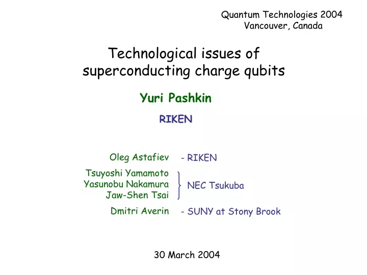
NEC Tsukuba. Quantum Technologies 2004 Vancouver, Canada. Technological issues of superconducting charge qubits. Yuri Pashkin. RIKEN. Oleg Astafiev Tsuyoshi Yamamoto Yasunobu Nakamura Jaw-Shen Tsai Dmitri Averin. - RIKEN. - SUNY at Stony Brook. 30 March 2004. Outline.

E N D
NEC Tsukuba Quantum Technologies 2004 Vancouver, Canada Technological issues of superconducting charge qubits Yuri Pashkin RIKEN Oleg Astafiev Tsuyoshi Yamamoto Yasunobu Nakamura Jaw-Shen Tsai Dmitri Averin - RIKEN - SUNY at Stony Brook 30 March 2004
Outline • introduction • electrostatic coupling • single-shot readout • T1 and T2 measurement • technological issues
Cooper-pair box M. Büttiker, 1987 V. Bouchiat et al, 1995 • a single artificial two-level system • ~108 conduction electrons in the box E = (CgVg – 2ne)2/2C box reservoir Cooper-pair tunneling - - - - n=0 1 ++++ gate
charge states: , coherent oscillations initial state Charge qubit based on Cooper-pair box Y. Nakamura et al, 1999 eigenstates: energy EJ gate voltage initialization coherent superposition read-out final state
e e + probe Final state read-out Josephson-quasiparticle cycle (Fulton et al., 1989) 2e Cooper-pair box • detect the state • initialize the system to
reservoir 2 reservoir 1 probe 1 probe 2 qubit 2 qubit 1 Cross Section dc gate 1 dc gate 2 pulse gate (common) box 2 box 1 1 m capacitive coupling I2 I1 Vb2 Vb1 Vg2 Vp Vg1 Capacitively coupled charge qubits standard e-beam lithography + angle evaporation I1 and I2 give info on charge states
I00> I10> I01> I11> I00> I10> I01> I11> Hamiltonian charge basis EJ1,2 ~ Em < Ec1,2 initial state I00> Ec1, Ec2, Em EJ1, EJ2 En1n2= Ec1(ng1–n1)² + Ec2(ng2–n2)² + Em(ng1–n1)(ng2–n2) Ec1,2= 4e²CΣ2,1/2(CΣ1,2CΣ2,1 – Cm²) 4e²CΣ2,1/2CΣ1,2CΣ2,1 ng1,2= (Cg1,2Vg1,2 + CpVp)/2e Em= 4e²Cm/(CΣ1CΣ2 – Cm2)
Oscillations at the double degeneracy E00 = E11 E10 = E01 0,0 I2 I1 1,0 0,1 dc gate1 dcgate2 1,1 pulse gate ng1 (= ng2) ng2 time 1,1 1 0,1 0.5 X superposition of four charge states! 0 1,0 0,0 ng1 1 0.5 0
Quantum beatings p1 p2 time, ps 0 1000 - - + + 2 2 operation point ng1 (= ng2) 0.5 0.45 2f
Quantum beatings: experiment 2.5 ns 0.6 ns EJ1 ng2 1,1 1 0,1 X EJ2 0.5 L R 0 1,0 0,0 ng1 1 0.5 - 0 + theoretically expected EJ1 = 13.4 GHz EJ2 = 9.1 GHz Em = 15.7 GHz
Single-shot readout EJ EJ trap+SET readout conventional readout qp = 0 qp ~ 1/10 ns trap kept unbiased during coherent evolution no qp relaxation! 2( + Ec) reservoir reservoir probe permanently biased! box box
Trap + SET readout box + trap galvanically isolated from the leads! no qp relaxation! no effect of the leads!
derivative of SET signal control+readout SET signal Time trace
Single-shot readout: coherent oscillations dead zones degeneracy
Relaxation of coherent oscillations no increase in T2
T1 measurement E • create 1 state by NA -pulse • move slowly along the upper band • stay for time • move slowly back • repeat for different ng -pulse with probability exp(-/T1) time
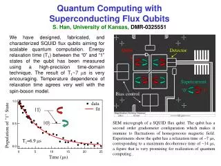
Superconducting charge qubits readout group control substrate T1 T2 dc probe NEC pulse pulse probe SiNx 5 ns 5 ns trap+SET switching current 1.8 s 0.5 s SiO2 -waves Saclay 1 s SiNx 100 ns pulse SiO2 Chalmers RF-SET 5 ns 5 ns
What next? 1. Qubit readout: dc probe pulsed probe trap + SET 2. Qubit control: NA pulses -waves 3. Materials: qubit Al Nb? substrate SiNx SiO2 4. Dependence of T1 and T2 on (1-3)
Nb SET Nb lead Nb island AlOx Barrier