Download
1 / 21
460 likes | 1.66k Views
The PIC Microcontrollers . The PIC microcontroller was designed by General Instruments The PIC microcontroller is a complete computer contained within one chip It contains the CPU, memory and IO devices all in one chip The microcontroller contains many IO ports such as PORTA, B, C, D, E

E N D
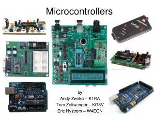
The PIC Microcontrollers • The PIC microcontroller was designed by General Instruments • The PIC microcontroller is a complete computer contained within one chip • It contains the CPU, memory and IO devices all in one chip • The microcontroller contains many IO ports such as PORTA, B, C, D, E • It contains also timers, analog to digital converter, USART • This make this device an ideal solution for small project 1
MEMORY ORGANIZATION • There are three memory blocks in each of the PIC16F87A devices • The program memory • The data memory • Stack memory • The program memory and data memory have separate buses which allows concurrent access 2
Program Memory Organization • The PIC microcontroller contains many internal registers to control its operation • One of these registers is the program counter • The program counter is 13-bits wide in the 16F877A microcontrollers • This limits the program memory space to 213=8k words×14 bits of flash program memory • When the microprocessor is first powered up it starts execution at memory location 0000H • When an interrupt occurs the microprocessor goes to memory location 0004H 3
Data Memory Organization • The data memory is partitioned into multiple banks which contains • The General Purpose Registers • The Special Function Registers 5
Data Memory Organization • A given bank is selected by bits RP1 (Status<6>) and RP0 (Status<5>) according to the table shown below • These two bits are located in the status register which is equivalent to the flag register found in the 8086 6
SPECIAL FUNCTION REGISTERS • The Special Function Registers are registers used by the CPU and peripheral modules for controlling the desired operation of the device • These registers are shown in the attached sheets • The most important registers will be discussed next
Status Register • The Status register contains the flag bits, reset status and the bank select bits for data memory
OPTION_REG Register • This register contains various control bits to configure • the TMR0 prescaler/WDT postscaler (single assignable • register known also as the prescaler), the external • INT interrupt, TMR0 and the weak pull-ups on PORTB
INTCON Register • This register is responsible controlling hardware interrupts • The GIE (bit 7) is responsible for enable or disable of all interrupts in the system • If GIE is 1 then all interrupts will be enabled otherwise all interrupts will be disabled • A complete description of these interrupts will be provided in the next slide
PIE1 Register • The PIE1 register contains the individual enable/disable bits for the peripheral interrupts • Peripherals are • the analog to digital converter • USART receiver • USART transmitter • Synchronous Serial Port • Timer1 • Timer2
PIR1 Register • When an interrupt is generated, it is important to know which one of the above mentioned peripherals generates the interrupt • This can be done by inspecting the state of the PIR1 register which contains several flag bits corresponds to each peripheral • If an interrupt occurs, then the program can test the flags located in this register to determine which device generated the interrupt • A complete explanation for this register is provided in the next slide
PCON Register • The Power Control (PCON) register contains flag bits to allow differentiation between a Power-on Reset (POR), a Brown-out Reset (BOR), a Watchdog Reset (WDT) and an external MCLR Reset