Download
1 / 35
350 likes | 482 Views
Efficient Thermal Placement of Standard Cells in 3D ICs using a Force Directed Approach. Brent Goplen, Sachin Sapatnekar Department of Electrical and Computer Engineering University of Minnesota. Overview. What are 3D ICs? Benefits of 3D integration Obstacles to 3D integration

E N D
Efficient Thermal Placement of Standard Cells in 3D ICs using a Force Directed Approach Brent Goplen, Sachin Sapatnekar Department of Electrical and Computer Engineering University of Minnesota
Overview • What are 3D ICs? • Benefits of 3D integration • Obstacles to 3D integration • Thermal issues • Reducing thermal problems • Finite Element Analysis (FEA) • Efficient temperature calculation • Force-directed placement • Thermal directed forces • Results • Conclusions
Layer 5 Layer 4 Layer 3 Layer 2 Layer 1 Bulk Substrate 3D IC Using Wafer Bonding Detailed view Generalized view SOI wafers with bulk substrate removed Inter-layer bonds 1mm Bulk wafer Metal level of wafer 1 10mm 500mm Device level 1 Adapted from [Das et al., ISVLSI, 2003]
3D ICs • Multiple active layers • Fabrication technologies • MCM-V • Single die • Recrystallization • Wafer bonding • Inter-layer interconnects
3D Global Net Distributions 1400 1200 4 Strata 2 Strata 1000 1 Stratum 800 Net Density (#/mm) 600 400 200 0 0 5 10 15 20 25 30 35 Length (mm) Performance Improvement of 3D ICs • Reduced wirelength • Total wirelength • Longest wirelength • More layers produce more improvement • Larger circuits produce more improvement • Lower power per transistor • Decreased interconnect delay • Higher transistor packing densities • Smaller chip areas [Joyner, Zarkesh-Ha and Meindl, ASIC/SOC ’01]
3D IC Obstacles • Processing technology • Thermal issues • More pronounced in 3D ICs • Higher power densities • Farther heat conduction paths • Insulating materials between layers • Thermal problems • Variations in performance • Reliability problems • Chip failure • 3D design tools from Intel
Minimize total power • Integration technology • Minimize wirelength • Improved heat removal • Packaging • Thermal vias • Evenly distribute heat • May not produce even temperature distribution • Manually fix hot spots • Lacking automation • Thermal placement • Minimize temperatures directly Methods of Mitigating Thermal Problems
Minimize total power • Integration technology • Minimize wirelength • Improved heat removal • Packaging • Thermal vias • Evenly distribute heat • May not produce even temperature distribution • Manually fix hot spots • Lacking automation • Thermal placement • Minimize temperatures directly Methods of Mitigating Thermal Problems
Minimize total power • Integration technology • Minimize wirelength • Improved heat removal • Packaging • Thermal vias • Evenly distribute heat • May not produce even temperature distribution • Manually fix hot spots • Lacking automation • Thermal placement • Minimize temperatures directly Methods of Mitigating Thermal Problems
Minimize total power • Integration technology • Minimize wirelength • Improved heat removal • Packaging • Thermal vias • Evenly distribute heat • May not produce even temperature distribution • Manually fix hot spots • Lacking automation • Thermal placement • Minimize temperatures directly Methods of Mitigating Thermal Problems
Minimize total power • Integration technology • Minimize wirelength • Improved heat removal • Packaging • Thermal vias • Evenly distribute heat • May not produce even temperature distribution • Manually fix hot spots • Lacking automation • Thermal placement • Minimize temperatures directly Methods of Mitigating Thermal Problems
Previous Work in Thermal Placement • Chu and Wong, ISPD, 1997 • Matrix synthesis method • Tsai and Kang, TCAD, 2000 • Finite difference method (FDM) • Simulated annealing method • Chen and Sapatnekar, ISPD, 2003 • Improved upon Tsai and Kang’s FDM method • Partitioning-based method • Previous work lacks efficiency and focused on 2D ICs
Efficient Thermal Placement Finite Element Analysis Thermal Forces Matrix Reduction Sparse Linear Solver Force Directed Placement
Temperature Calculation T is the temperature Kx, Ky, and Kz are the thermal conductivities in the x, y, and z directions Q is the heat generated per unit volume • Heat transfer differential equation: • Unique solution with boundary conditions applied • No closed form solution for complex structures • Numerically solved
Produce an element matrix for each element Construct the global matrix using the element matrices Reduce the global matrix using boundary conditions Solve using a sparse linear solver Finite Element Analysis (FEA) Discretize (mesh) the entire structure into elements
Inter-layer elements Layer elements Standard cells (heat sources) Bulk substrate elements FEA Mesh of the 3D IC
4 3 7 8 2 1 h d y w 6 5 x z Element Stiffness Matrix • Stamp for a hexahedral element • Rows and columns correspond to nodes 1 - 8
Element and Global Matrices • Elements are aligned in a grid pattern • Element matrices, [k], are calculated for each element • Similar to the Modified Nodal Formulation: • These stamps, [k], are added to the global matrix, [Kglobal] • [Kglobal]{T} = {P} • {P} is the power and {T} are the temperatures
Element Assembly Example d 7 g 8 9 a 4 b 5 6 1 2 3
Element Assembly Example d 7 g 8 9 a 4 b 5 6 1 2 3
Element Assembly Example d 7 g 8 9 a 4 b 5 6 1 2 3
Element Assembly Example d 7 g 8 9 a 4 b 5 6 1 2 3
Reducing the Global Matrices using Fixed Temperatures and Positions • Starting with a global system of equations • X1 are the unknown values • X2 are fixed values • Eliminate rows and columns corresponding to fixed values • Results in a reduced system of equation • Applicable to both FEA and force-directed methods
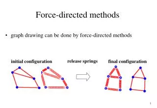
Cell 3 IOPad 1 Cell 4 Net1 Net2 Cell 1 IOPad 2 Net3 Cell 5 Cell 2 Force-directed model Star net representation Spring forces attracts connected cells together IOPad 1 Cell3 Cell4 Net2 Cell1 IOPad 2 Net3 Cell2 Cell5
Force-Directed Placement Methods • Cost of a connection between two nodes: • Objective function to minimize: • Solve the following systems of equations:
Force-Directed Placement Stamp • The following stamp is created for each net and added to [C] • Repulsive cell forces, {Fx, Fy, Fz}, are added to the systems of equations,
Thermal Gradient Forces • Used to drive cells apart in hot spots • Magnitude, direction determined by thermal gradient 1 3 2 4 5 6 7
Repulsive Forces • The repulsive forces are composed of: • thermal-dependent components • overlap-dependent components • {ftherm} based on thermal gradient • {fove} based on Eisenmann and Johannes, DAC, 1998 • krep adjusted between iterations to balance forces • {frep} used to update repulsive forces {Fx, Fy, Fz} • {Fx, Fy, Fz} added to total forces: {fx}, {fy}, and {fz} • OP is the percent contribution from overlap forces
RANDOM PLACEMENT CALCULATE TEMPERATURES DETERMINE THERMAL FORCES Main loop DETERMINE OVERLAP FORCES CALCULATE NEW POSITIONS CONVERGED? NO YES POST-PROCESS Thermal Placement Algorithm CONSTRUCT NET AND THERMAL MATRICES
Post-Processing • Place cells into the nearest layer • Put excess cells into adjacent layers • Place cells into the nearest row • Put excess cells into adjacent rows • A divide and conquer approach is used to remove overlap within each row • Sort cells in the x direction and divide into two group • Remove overlap during division • Continue recursively until all overlap is removed
Benchmark Results • 1.3% reduction in the average temperature, Tave • 12% reduction in the maximum temperature, Tmax • 17% reduction in the average thermal gradient, gave • 5.5% increase in the total wirelength, Ltotal
Thermal Placement for ibm01Using a Skewed Power Distribution Temperature Profile Power Profile • 20% lower average temperature and 54% lower maximum temperature • 78% lower average thermal gradient and 10% longer wirelengths
Conclusions • Thermal issues more prominent in 3D ICs • Thermal placement mitigates thermal problems • FEA used for temperature calculation • Thermal forces move cells away from hot spots • Linear efficiency to handle increasing circuit sizes • Optimization of both temperature and wirelength