Download
1 / 6

E N D
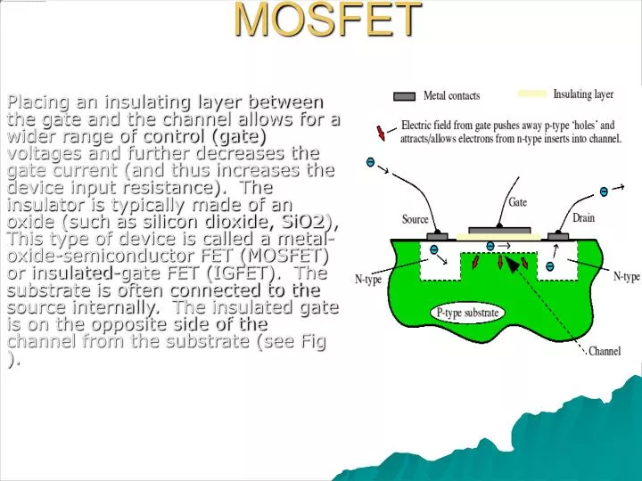
MOSFET Placing an insulating layer between the gate and the channel allows for a wider range of control (gate) voltages and further decreases the gate current (and thus increases the device input resistance). The insulator is typically made of an oxide (such as silicon dioxide, SiO2), This type of device is called a metal-oxide-semiconductor FET (MOSFET) or insulated-gate FET (IGFET). The substrate is often connected to the source internally. The insulated gate is on the opposite side of the channel from the substrate (see Fig ).
MOSFET The bias voltage on the gate terminal either attracts or repels the majority carriers of the substrate across the PN junction with the channel. This narrows (depletes) or widens (enhances) the channel, respectively, as VGS changes polarity. For N-channel MOSFETs, positive gate voltages with respect to the substrate and the source (VGS > 0) repel holes from the channel into the substrate, thereby widening the channel and decreasing channel resistance. Conversely, VGS < 0 causes holes to be attracted from the substrate, narrowing the channel and increasing the channel resistance. Once again, the polarities discussed in this example are reversed for P-channel devices. The common abbreviation for an N-channel MOSFET is NMOS, and for a P-channel MOSFET, PMOS.
MOSFET Because of the insulating layer next to the gate, input resistance of a MOSFET is usually greater than 1012 Ohms (a million megohms). Since MOSFETs can both deplete the channel, like the JFET, and also enhance it, the construction of MOSFET devices differs based on the channel size in the resting state, VGS = 0. A depletion mode, device (also called a normally on MOSFET) has a channel in resting state that gets smaller as a reverse bias is applied, this device conducts current with no bias applied (see Fig ). An enhancement mode device (also called a normally off MOSFET) is built without a channel and does not conduct current when VGS = 0; increasing forward bias forms a channel that conducts current (see Fig. ).
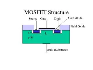
n-type Metal-Oxide-Semiconductor-Field-Effect-Transistor (MOSFET) The n-type Metal-Oxide-Semiconductor Field-Effect-Transistor (nMOSFET) consists of a source and a drain, two highly conducting n-type semiconductor regions, which are isolated from the p-type substrate by reversed-biased p-n diodes. A metal or poly-crystalline gate covers the region between source and drain. The gate is separated from the semiconductor by the gate oxide. The basic structure of an n-type MOSFET and the corresponding circuit symbol are shown in Figure shown.
N-Type MOSFET • A top view of the same MOSFET is shown in Figure 2, where the gate length, L, and gate width, W, are identified. Note that the gate length does not equal the physical dimension of the gate, but rather the distance between the source and drain regions underneath the gate. The overlap between the gate and the source/drain region is required to ensure that the inversion layer forms a continuous conducting path between the source and drain region. Typically this overlap is made as small as possible in order to minimize its parasitic capacitance