Download
1 / 33
550 likes | 1k Views
Chap. 8. Central Processing Unit. 2007.05.01. Agenda. 8.1 Introduction 8.2 General Register Organization 8.3 Stack Organization 8.4 Instruction Formats 8.5 Addressing Modes 8.6 Data Transfer and Manipulation 8.7 Program Control 8.8 Reduced Instruction Set Computer.

E N D
Chap. 8. Central Processing Unit 2007.05.01
Agenda 8.1 Introduction 8.2 General Register Organization 8.3 Stack Organization 8.4 Instruction Formats 8.5 Addressing Modes 8.6 Data Transfer and Manipulation 8.7 Program Control 8.8 Reduced Instruction Set Computer
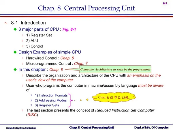
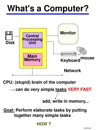
8.1 Introduction (1/2) • CPU • CPU (Central Processing Unit) : the part of the computer that performs the bulk of data-processing operations • 3 major part of CPU: Fig. 8-1 1) Register set: stores intermediate data used during the execution of the instruction 2) ALU(Arithmetic Logic Unit): performs the required microoperations for executing the instruction 3) Control Unit: supervises the transfer of information among the register and instructs the ALU as to which operation to perform 2014-09-21 컴퓨터기본구조-Chap.8 3
8.1 Introduction (2/2) • CPU • Design Examples of simple CPU - Hardwired Control : Chap. 5 - Microprogrammed Control : Chap. 7 • In this chapter : Chap. 8 - Describe the organization and architecture of the CPU with an emphasis on the user’s view of the computer - User who programs the computer in machine/assembly language must be aware of 1) Instruction Formats 2) Addressing Modes 3) Register Sets - The last section presents the concept of Reduced Instruction Set Computer (RISC) 2014-09-21 컴퓨터기본구조-Chap.8 4
Agenda 8.1 Introduction 8.2 General Register Organization 8.3 Stack Organization 8.4 Instruction Formats 8.5 Addressing Modes 8.6 Data Transfer and Manipulation 8.7 Program Control 8.8 Reduced Instruction Set Computer
8.2 General Register Organization (1/7) • Register의 필요성 • Memory locations are needed for storing pointers, counters, return address, temporary results, and partial products during multiplication (in the Programming examples of Chap. 6) • Memory access is the most time-consuming operation in a computer • More convenient and efficient way is to store intermediate values in processor registers 2014-09-21 컴퓨터기본구조-Chap.8 6
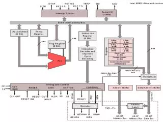
8.2 General Register Organization (2/7) • Bus organization for 7 CPU registers : Fig. 8-2 • 2 MUX : select one of 7 register or external data input by SELA and SELB • BUS A and BUS B: form the inputs to a common ALU • ALU : OPR determine the arithmetic or logic microoperation • The result of the microoperation is available for output data and also goes into the inputs of all the registers • 3 X 8 Decoder : select the register (by SELD) that receives the information from ALU 2014-09-21 컴퓨터기본구조-Chap.8 7
8.2 General Register Organization (3/7) • Binary Selector input • Example: R1 ← R2 + R3 • MUX A selector (SELA) : to place the content of R2 into BUS A • MUX B selector (SELB) : to place the content of R3 into BUS B • ALU operation selector (OPR) : to provide the arithmetic addition R2 + R3 • Decoder selector (SELD) : to transfer the content of the output bus into R1 2014-09-21 컴퓨터기본구조-Chap.8 8
8.2 General Register Organization (4/7) • Control Word • 14 bit control word(4 fields): Fig. 8-2(b) • SELA (3 bits) : select a source register for A input of the ALU • SELB (3 bits) : select a source register for B input of the ALU • SELD (3 bits) : select a destination register using the 3 X 8 decoder • OPR (5 bits) : select one of the operation in the ALU 2014-09-21 컴퓨터기본구조-Chap.8 9
8.2 General Register Organization (5/7) • Control Word • Encoding of Register Selection Fields: Tab. 8-1 • SELA or SELB = 000 (Input): MUX selects the external input data • SELD = 000 (None): no destination register is selected but the contents of the output bus are available in the external output 2014-09-21 컴퓨터기본구조-Chap.8 10
8.2 General Register Organization (6/7) • Control Word • Encoding of ALU Operation (OPR): Tab. 8-2 2014-09-21 컴퓨터기본구조-Chap.8 11
8.2 General Register Organization (7/7) • Control Word • Example of Microoperation Tab. 8-3 → Control Word를 Control Memory에 저장하여 Microprogrammed Control 방식으로 제어 가능함 2014-09-21 컴퓨터기본구조-Chap.8 12
Agenda 8.1 Introduction 8.2 General Register Organization 8.3 Stack Organization 8.4 Instruction Formats 8.5 Addressing Modes 8.6 Data Transfer and Manipulation 8.7 Program Control 8.8 Reduced Instruction Set Computer
8.3 Stack Organization (1/6) • Stack or LIFO(Last-In, First-Out) • A Storage device that stores information • The item stored last is the first item retrieved = a stack of tray • Stack Pointer (SP) • The register that holds the address for the stack • SP always points at the top item in the stack • Two Operations of a stack : Insertion and Deletion of Items • PUSH : Push-Down = Insertion • POP : Pop-Up = Deletion • Stack의 종류 • Register Stack (Stack Depth가 제한) • a finite number of memory words or register(stand alone) • Memory Stack (Stack Depth가 유동적) • a portion of a large memory 2014-09-21 컴퓨터기본구조-Chap.8 14
8.3 Stack Organization (2/6) • Register Stack: Fig. 8-3 • 64-word stack : stack pointer : 6 bit(0~63) , 26=64 • FULL : In the case of SP=63, Push Operation, then SP=0 : SP = 63+1 = 111111 + 1 = 1000000 = 0 (X) FULL ← 1 • EMPTY : In the case of SP=0, POP Operation, then SP=63 : SP = 0 – 1 = 000000 – 1 = 111111 (X) EMPTY ← 1 • DR : the data register that holds the binary data to written into or read out of the stack. 2014-09-21 컴퓨터기본구조-Chap.8 15
8.3 Stack Organization (3/6) • Register Stack: Fig. 8-3 • 초기 조건 : SP=0, EMTY=1, FULL=0 • PUSH : If the stack is not full (if FULL=0), new item is inserted with a push operation SP ← SP + 1 Increment stack pointer M[SP] ← DR Write item on top of the stack if (SP=0) then (FULL ← 1) Check if stack is full EMPTY ← 0 Mark the stack not empty • POP : A new item is deleted from stack if the stack is not empty (if EMTY=0) DR ← M[SP] Read item from the top of stack SP ← SP – 1 Decrement stack pointer if (SP=0) then (EMTY ← 1) Check if stack if empty FULL ← 0 Mark the stack not full 2014-09-21 컴퓨터기본구조-Chap.8 16
8.3 Stack Organization (4/6) • Memory Stack: Fig. 8-4 : a portion of computer memory partitioned into three segments: program, data and stack. • 초기 조건 : SP=4001 : stack grows with decreasing addresses • PUSH SP ← SP - 1 M[SP] ← DR • POP DR ← M[SP] SP ← SP + 1 2014-09-21 컴퓨터기본구조-Chap.8 17
8.3 Stack Organization (5/6) • Memory Stack: Fig. 8-4 • Stack Limits - Check for stack overflow(full)/underflow(empty) - Checked by using two register . Upper Limit and Lower Limit Register . After PUSH Operation > SP compared with the upper limit register . After POP Operation > SP compared with the lower limit register • Stack Limits : Fig. 8-4 : upper limit register = 3000 : lower limit register = 4001 을 이용 • Error Condition : PUSH when FULL = 1 : POP when EMTY = 1 2014-09-21 컴퓨터기본구조-Chap.8 18
8.3 Stack Organization (6/6) • RPN(Reverse Polish Notation) • Arithmetic Expression: A + B • A + B Infix Notation • + A B Prefix Polish Notation • A B + Postfix or Reverse Polish Notation • The reverse Polish notation is very suitable for stack manipulation • 예제) A * B + C * D AB * CD * + : Fig. 8-5 • ( 3 * 4 ) + ( 5 * 6 ) 3 4 * 5 6 * + 2014-09-21 컴퓨터기본구조-Chap.8 19
Agenda 8.1 Introduction 8.2 General Register Organization 8.3 Stack Organization 8.4 Instruction Formats 8.5 Addressing Modes 8.6 Data Transfer and Manipulation 8.7 Program Control 8.8 Reduced Instruction Set Computer
8.4 Instruction Formats (1/5) • Instruction Field • Operation Code Field : specify the operation to be performed • Address Field : designate a memory address or a processor register • Mode Field : specify the operand or the effective address (Addressing Mode) • The number of address fields in the instruction format of a computer depends on the internal organization of its registers • Three type of CPU organization • Single accumulator organization ex) ADD X /* AC ← AC + M[X] */ • General register organization ex) ADD R1, R2, R3 /* R1 ← R2 + R3 */ ADD R1, R2 /* R1 ← R1 + R2 */ MOV R1, R2 /* R1 ← R2 */ ADD R1, X /* R1 ← R1 + M[X] */ • Stack organization ex) PUSH X /* TOS ← M[X] ADD 2014-09-21 컴퓨터기본구조-Chap.8 21
8.4 Instruction Formats (2/5) • The Influence of the number of addresses on computer instruction • [예제] X = ( A + B ) * ( C + D ) • 4 arithmetic operations : ADD, SUB, MUL, DIV • 1 transfer operation to and from memoryand general register : MOV • 2 transfer operation to and from memory and AC register : STORE, LOAD • Operand memory addresses : A, B, C, D • Result memory address : X 2014-09-21 컴퓨터기본구조-Chap.8 22
8.4 Instruction Formats (3/5) • Three-Address Instructions • Program to evaluate: X = ( A + B ) * ( C + D ) ADD R1, A, B /* R1 ← M[A] + M[B] */ ADD R2, C, D /* R2 ← M[C] + M[D] */ MUL X, R1, R2 /* X ← R1 * R2 */ • (+) result in short programs when evaluating arithmetic expression • (-) binary-coded instructions require too many bits to specify three address • Two-Address Instructions • Program to evaluate: X = ( A + B ) * ( C + D ) MOV R1, A /* R1 ← M[A] */ ADD R1, B /* R1 ← R1 + M[B] */ MOV R2, C /* R2 ← M[C] */ ADD R2, D /* R2 ← R2 + M[D] */ MUL R1, R2 /* R1 ← R1 * R2 */ MOV X, R1 /* M[X] ← R1 */ • The most common in commercial computers • Each address fields specify either a processor register or a memory operand 2014-09-21 컴퓨터기본구조-Chap.8 23
8.4 Instruction Formats (4/5) • One-Address Instructions • use an implied accumulator(AC) register for all data manipulation • Program to evaluate: X = ( A + B ) * ( C + D ) LOAD A /* AC ← M[A] */ ADD B /* AC ← AC + M[B] */ SOTRE T /* M[T] ← AC */ LOAD C /* AC ← M[C] */ ADD D /* AC ← AC + M[D] */ MUL T /* AC ← AC * M[T] */ SOTRE X /* M[X] ← AC */ • All operations are done between the AC register and memory operand • Zero-Address Instructions • can be found in a stack-organized computer • Program to evaluate: X = ( A + B ) * ( C + D ) PUSH A /* TOS ← A */ PUSH B /* TOS ← B */ ADD /* TOS ← (A + B) */ PUSH C /* TOS ← C */ PUSH D /* TOS ← D */ ADD /* TOS ← (C + D) */ MUL /* TOS ← (C + D) * (A + B) */ POP X /* M[X] ← TOS */ 2014-09-21 컴퓨터기본구조-Chap.8 24
8.4 Instruction Formats (5/5) • RISC Instruction • Reduced Instruction Set Computer(RISC) • Only use LOAD and STORE instruction when communicating between memory and CPU • All other instructions are executed within the registers of the CPU without referring to memory • RISC architecture will be explained in Sec. 8-8 • Program to evaluate: X = ( A + B ) * ( C + D ) LOAD R1, A /* R1 ← M[A] */ LOAD R2, B /* R2 ← M[B] */ LOAD R3, C /* R3 ← M[C] */ LOAD R4, D /* R4 ← M[D] */ ADD R1, R1, R2 /* R1 ← R1 + R2 */ ADD R3, R3, R4 /* R3 ← R3 + R4 */ MUL R1, R1, R3 /* R1 ← R1 * R3 */ STORE X, R1 /* M[X] ← R1 */ 2014-09-21 컴퓨터기본구조-Chap.8 25
Agenda 8.1 Introduction 8.2 General Register Organization 8.3 Stack Organization 8.4 Instruction Formats 8.5 Addressing Modes 8.6 Data Transfer and Manipulation 8.7 Program Control 8.8 Reduced Instruction Set Computer
8.5 Addressing Modes (1/6) • Addressing Mode의 필요성 • To give programming versatility to the user • pointers to memory, counters for loop control, indexing of data, … • To reduce the number of bits in the addressing field of the instruction • Instruction Cycle • Fetch the instruction from memory and PC + 1 • Decode the instruction • Execute the instruction • Program Counter (PC) • PC keeps track of the instructions in the program stored in memory • PC holds the address of the instruction to be executed next • PC is incremented each time an instruction is fetched from memory • Addressing Mode of the Instruction • Distinct Binary Code • Instruction Format 에 Opcode 와 같이 별도에 Addressing Mode Field를 갖고 있음 • Single Binary Code • Instruction Format에 Opcode 와 Addressing Mode Field가 섞여 있음 • Instruction Format with mode field: Fig. 8-6 2014-09-21 컴퓨터기본구조-Chap.8 27
8.5 Addressing Modes (2/6) • Implied Mode • Operands are specified implicitly in definition of the instruction • Examples • COM: Complement Accumulator • Operand in AC is implied in the definition of the instruction • PUSH: Stack push • Operand is implied to be on top of the stack • Immediate Mode • Operand field contains the actual operand • Useful for initializing registers to a constant value • Examples : LD #NBR /* AC ← NBR */ • Register Mode • Operands are in registers • Register is selected from a register field in the instruction • k-bit register field can specify any one of 2k registers • Examples : LD R1 /* AC ← R1 */ 2014-09-21 컴퓨터기본구조-Chap.8 28
8.5 Addressing Modes (3/6) • Register Indirect Mode • Selected register contains the address of the operand rather than the operand itself • Address field of the instruction uses fewer bits to select a memory address • Register 를 select 하는 것이 bit 수가 적게 소요됨 • Example : LD (R1) /* AC ← M[R1] */ • Autoincrement or Autodecrement Mode • Similar to the register indirect mode except that • the register isincremented afterits value is used to access memory • the register isdecrement beforeits value is used to access memory • Example (Autoincrement) : LD (R1)+ /* AC ← M[R1], R1 ← R1 +1 */ • Direct Addressing Mode • Effective address is equal to the address field of the instruction (Operand) • Address field specifies the actual branch address in a branch-type instruction • Example : LD ADR /* AC ← M[ADR] */ 2014-09-21 컴퓨터기본구조-Chap.8 29
8.5 Addressing Modes (4/6) • Indirect Addressing Mode • Address field of instruction gives the address where the effective address is stored in memory • Example : LD @ADR /* AC ← M[M[ADR]] */ • Relative Addressing Mode • PC is added to the address part of the instruction to obtain the effective address • Example : LD $ADR /* AC ← M[PC+ADR] */ • Indexed Addressing Mode • XR (Index register) is added to the address part of the instruction to obtain the effective address • Example : LD ADR(XR) /* AC ← M[ADR+XR] */ 2014-09-21 컴퓨터기본구조-Chap.8 30
8.5 Addressing Modes (5/6) • Base Register Addressing Mode • the content of a base register is added to the address part of the instruction to obtain the effective address • Similar to the indexed addressing mode except that the register is now called a base register instead of an index register • index register (XR) : LD ADR(XR)/* AC ← M[ADR+XR] */ • index register hold an index number that is relative to the address part of the instruction • base register (BR) : LD ADR(BR) /* AC ← M[BR+ADR] */ • base register hold a base address • the address field of the instruction gives a displacement relative to this base address 2014-09-21 컴퓨터기본구조-Chap.8 31
8.5 Addressing Modes (6/6) • Numerical Example: Fig. 8-6 500 + 202 (PC) R1 = 400 (after) 500 + 100 (XR) R1 = 400 -1 (prior) R1 = 400 2014-09-21 컴퓨터기본구조-Chap.8 32
Homework • 8-7, 14, 18 2014-09-21 컴퓨터기본구조-Chap.8 33