Download
1 / 10
120 likes | 467 Views
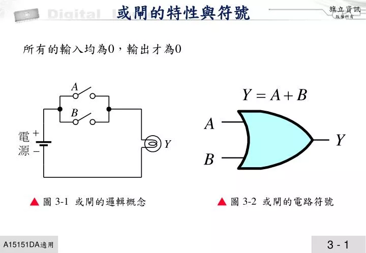
或閘的特性與符號. 所有的輸入均為 0 ,輸出才為 0. ▲ 圖 3-2 或閘的電路符號. ▲ 圖 3-1 或閘的邏輯概念. 或閘的電路結構與真值表. ▼ 表 3-1 或閘的真值表. ▲ 圖 3-3 或閘的電路結構. 及閘的特性與符號. 所有的輸入均為 1 ,輸出才為 1. ▲ 圖 3-5 及閘的電路符號. ▲ 圖 3-4 及閘的邏輯概念. 及閘的電路結構與真值表. ▼ 表 3-2 及閘的真值表. ▲ 圖 3-6 及閘的電路結構. 反閘的特性與符號. ▲ 圖 3-8 反閘的電路符號.

E N D
或閘的特性與符號 所有的輸入均為0,輸出才為0 ▲圖 3-2 或閘的電路符號 ▲圖 3-1 或閘的邏輯概念
或閘的電路結構與真值表 ▼表3-1 或閘的真值表 ▲圖 3-3 或閘的電路結構
及閘的特性與符號 所有的輸入均為1,輸出才為1 ▲ 圖 3-5 及閘的電路符號 ▲圖 3-4 及閘的邏輯概念
及閘的電路結構與真值表 ▼表3-2 及閘的真值表 ▲圖 3-6 及閘的電路結構
反閘的特性與符號 ▲圖 3-8 反閘的電路符號 ▲圖 3-7 反閘的邏輯概念
反閘的電路結構與真值表 (a)基本電路 (b)改良後的電路 ▲圖 3-9 反閘的電路結構 ▼表3-3 反閘的真值表
反或閘的符號與真值表 所有的輸入均為0,輸出才為1 ▼表3-4 反或閘(NOR gate)與或閘 (OR gate)的真值表比較 ▲圖 3-10 反或閘的電路符號
反及閘的符號與真值表 所有的輸入均為1,輸出才為1 ▼表3-5 反及閘(NAND gate)與及閘 (AND gate)的真值表比較 ▲圖 3-12 反及閘的電路符號
互斥或閘的符號與真值表 兩輸入不同時,輸出才為1 ▼表3-5 互斥或閘的真值表比較 ▲圖 3-14 互斥或閘的電路符號
反互斥或閘的符號與真值表 兩輸入相同時,輸出才為1 ▼表3-5 反互斥或閘(XNOR gate)與互斥或閘(XOR gate)的真值表比較 ▲圖 3-15 反互斥或閘的電路符號