Download
1 / 34
340 likes | 474 Views
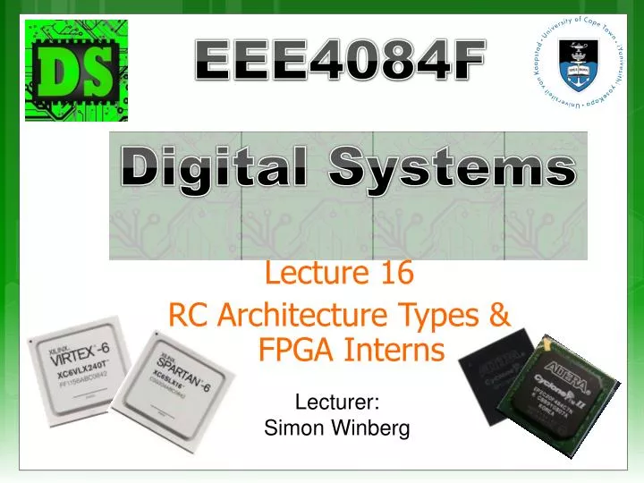
Lecture 16 RC Architecture Types & FPGA Interns. EEE4084F. Digital Systems. Lecturer: Simon Winberg. Reminders & YODA milestone dates Marking process RC Architecture overview & main types Recap of FPGAs. Lecture Overview. Form YODA project groups!!

E N D
Lecture 16 RC Architecture Types & FPGA Interns EEE4084F Digital Systems Lecturer: Simon Winberg
Reminders & YODA milestone dates Marking process RC Architecture overview & main types Recap of FPGAs Lecture Overview
Form YODA project groups!! Indicate your team in the Wiki. Add a blog entry to describe your topic Start on your project ASAP 7 May – Design Review Reminder
Projects done as teams of 2 or 3 • (confirm team of 1 or 3 with lecturer) • Milestone Dates • Blog (due 3 Apr) • Design review (todo list by 7 May) • Demo (16-17 May) • Code and final report (20 May) Project Teams & Marking
Early Notice: • Quiz 3 Thursday (25 Apr) • Held 2pm, 45 minutes • Covers • Lecture 12 – 16 • Seminar 7 (CH7), • Seminar 8 (CH14) Quiz next Thursday!
Assignment work is marked in relation to • Correctness • Completion • Structure, effectiveness of wording & layout • Adequate amount of detail/results shown & effectively dealing with the details • Indication of student’s understanding and engagement with the discipline • Clarity of explanations/motivation of results • Professionalism and overall quality Report Marking process
Structure & Effectiveness Note that a mark out of 10 is just an example, depending what the assignment is marked out of in total, and weighting for different sections, this can change 0 lower marks 10 higher marks Well structured; Clear progression; Logically structured; Clear and effective use of headings (if headings are requested); table of contents and clear title (if asked for) Cobbled together; List of points with no effort to formulate a logical structure or flow to the argument/results
Understanding 0 lower marks 10 higher marks Clear grasp of methods; Good discussion of techniques; Correct math and calculations; Good choices; Indication of scope; Clear / logical reasoning and motivation; Appropriate terminology Poor understanding; Over generalizing; Mathematical/logical mistakes; Non-critical discussion; Stating facts without adequate motivation
Correctness 0 lower marks 10 higher marks Correct answers; Well formulated proofs / correct explanations; Logical deductions used; Adequate evidence / proofs to support conclusions or generalized results Wrong answers; Many mistakes; Illogical results; Inadequate proof / evidence for presented conclusions or results.
Level of detail & Dealing with details 0 lower marks 10 higher marks An effective amount of detail. Using means, such as annotations and textual explanations, to bring out important results if a lot of data was given in the report. Too little detail … or perhaps an excessive amount that makes it difficult to make sense (for the maker) of what is being shown
Engagement with the discipline 0 lower marks 10 higher marks Effective use of discipline-specific terminology; effective use of techniques and knowledge that are well understood in the discipline. Elegant explanations using references were applicable. Using ineffective terminology. Ineffective techniques, e.g. inappropriate for the work concerned. Cumbersome explanations not building on well understand theories in the discipline.
Professionalism 0 lower marks 10 higher marks Elegant and easy-to-read layout; Good wording, well organized; Clear discussions and explanations; Proof-read; Good references (if needed); Cross-referencing to other parts of the document (if relevant); Consistent; Good grammar and correct spelling. Poor layout of documents; Inappropriate wording; Poor choice of fonts; Confusing discussions and explanations; Errors in symbols and units; Grammar and spelling mistakes; Inconsistencies
RC Architectures Overview Reconfigurable Computing
A determining factor is ability to change hardware datapaths and control flows by software control This change could be either a post-process / compile time or dynamically during runtime (doesn’t have to be both) Is it or isn’t it reconfigurable…? While the trivial case (a computer with one changeable datapath could be argued as being reconfigurable) it is usually assumed the computer system concerned has many changeable datapaths. processing elements Datapath
Currently there are two basic forms: • Microprocessor-based RC • FPGA-based RC RC Architectures • Microprocessor-based RC: • A few platform configurability features added to a microprocessor system (e.g., a multi-processor motherboard that can reroute the hardware links between processors) • Besides that we’ve already seen it all in the microprocessor parallelism in part of the course
Microprocessor based RC • Multi-core processors dynamicallyjoined to create a larger/smallerparallel system when needed • Assumed to be a single computer platform as apposed to a cluster of computers • Needs to support software-controlled dynamic reconfiguration (see previous slide) • Tends to become:Hardware essentially changeable in big blocks (“macro-level reconfiguration” - whole processors at a time) RC Architectures– basic forms
FPGA based • Generally much smaller level ofinterconnects (more at the “micro-level reconfiguration”) • Processors that connect to FPGA(s) RC Architectures– basic forms
Generally, these systems follow a processors + coprocessors arrangement • CPU connectors to reprogrammablehardware (usually FPGAs) • The CPU itself may beentirely in an FPGA • The lower-levelarchitecture is moreinvolved… topic of Seminar #7 (‘Interconnection Fabrics’) and further discussed in later lectures. General Architecture for using FPGA-based RC Multi-processor or multi-core processor computer CPU CPU … high-speed bus FPGA-based Accelerator card FPGA-based Accelerator card … Plug-in cards
FPGA Interns EEE4084F
FPGA internal structure Programmable logic element (PLE)(or FPLE*) Image adapted from Maxfield (2004) Note: one programmable logic block (PLB) may contain a complex arrangement of programmable logic elements (PLE). The size of a FPGA or programmable logic device (PLD) is measured in the number of LEs (i.e., Logic Elements) that it has. * FPLE = Field Programmable Logic Element
You already know all your logic primitives… • The primitive logic gates • AND, OR, NOR, NOT, NOR, NAND, XOR • AND3, OR4, etc (for multiple inputs). • Pins / sources / terminators • Ground, VCC • Input, output • Storage elements • JK Flip Flops • Latches • Others items: delay, mux Logic Elements– Remember your logic primitives OR Input Pin Output Pin Altera Quartus II representations
A simple but powerful approach to FPGA design is to use lookup tables for the PLBs. These are usually implemented as a combination of a multiplexer and memory (even just using NOR gates) Essentially, this approach is building complex circuits using truth tables (where each LUT enumerates a truth table) Look Up Tables (LUTs) The usual strategy for implementing PLBs examples follows…
Simple 3-LUT implementation for a PLB input values 0 000 001 1 010 1 0 011 1-bit output 1 100 0 Any guesses as to what logic circuit this LUT implements? 101 110 0 111 1 8-bit static memory 3 3-bit input bus
Simple 3-LUT implementation for a PLB It’s an XOR of the 3 input lines!!! input lines in out 0 000 output 001 1 010 1 0 011 1 100 0 101 0 110 111 1
Mainstream* Programmable Logic Block (PLB) Configure synchronous or asynchronous response (i.e. a line from another big LUT). config_sync k-input LUT 0 k inputs output DFF … 1 clock Another example for implementing an alternate logic function. Image adapted from Maxfield (2004) * Used by manufacturers like Xilinx
Logic block clusters (LBCs) and Configurable logic blocks (CLBs) • Assume a k-input LUT for each logic block (LB) • Assume N x LBs per logic cluster • BLEs in each logic clusters are fully connected or mostly connected The diagram shows the same input lines (I) are sent to each LB, in addition to each of the N LBs’ output lines. Each LB operates on 4 input lines at a time, and a MUX is used to decide which input to sample. The MUXs may be configured from a separate LUT, or could be controlled by the LB it is connected to. LB … N x LBs LB Diagram adapted from SheriefReda (2007), EN2911X Lecture 2 Fall07, Brown University
Xilinx L and M Slices Approachfor configurable logic blocks (CLBs) “Every slice contains four logic-function generators (or LUTs), eight storage elements, wide-function multiplexers, and carry logic. These elements are used by all slices to provide logic, arithmetic, and ROM functions. In addition to this, some slices support two additional functions: storing data using distributed RAM and shifting data with 32-bit registers. Slices that support these additional functions are called SLICEM; others are called SLICEL. SLICEM represents a superset of elements and connections found in all slices. Each CLB can contain zero or one SLICEM. Every other CLB column contains a SLICEMs. In addition, the two CLB columns to the left of the DSP48E columns both contain a SLICEL and a SLICEM.” Source: http://www.xilinx.com/support/documentation/user_guides/ug364.pdfpg 8
SLICEM slices support additional functions; they are a superset of SLICELs; i.e. the have all the standard LEs plus some additions. Source: http://www.xilinx.com/support/documentation/user_guides/ug364.pdf pg 9
SLICEL slices contain the standard set of LEs for the particular FPGA concerned. As the diagram shows, it looks a little less complicated than the design of a SLICEM. Source: http://www.xilinx.com/support/documentation/user_guides/ug364.pdf pg 10
HDL to FPGA execution & LE cost In order to implement a HDL design, the design need to be decomposed and mapped to the physical LBs on the FPGA and the interconnects need to be appropriately configured. Example: x = AND(e,f,g) y = AND(b,NAND(NAND(b,c),d)) out = NAND((NAND(x,y),NAND(a,y)) Map ‘AND(e,f,g)’ to LB1 Map ‘NAND((NAND(x,y),NAND(a,y))’ to LB2 x out y Map ‘AND(b,NAND(NAND(b,c),d)) ’ to LB3 Costing: 3 LBs, 8 LEs (assuming LBs have LEs that are AND or NAND gates)
The previous slide didn’t show whether the connections were synchronized (i.e., a shared clock) or asynchronous –since they are all logic gates and no clocks show it’s probably asynchronous Determining the timing constrains for synchronous configurations are generally easier, because everything is related to the clock speed. Still, you need to keep in mind cascading calculations. For asynchronous use, the implementation could run faster, but can also become a more complicated design, and be more difficult to work out the timing… Timing calculations
Keep in mind that the propagation delays for the various gates / LUTs may be different – for example, in the previous example, let’s assume each AND may take 6ns to stabilise, and the NANDS 10ns. So time to compute out is = Async Timing calculations MAX OF (time to compute x, time to compute y) + 2x10ns = (2x10ns+6ns) + 20ns = 46ns= pretty fast!! Or is it?? • Compared to a 1GHz CPU using just registers (and no mem access)? • Try this calculation for yourself ... • (assume each instruction takes on avg. 3 clocks due to pipeline, data dependencies, etc, as worst case performance on a RISC processor)
Comparing to CPU speed CPU running at 1GHz each clock 1ns period Assume each instruction takes ~ 5 clocks each due to pipeline etc CODE: intdoit ( unsigned a, b, c, d, e, f, g ) { unsigned x = AND(e,f,g); unsigned y = AND(b,NAND(NAND(b,c),d)) out = NAND((NAND(x,y),NAND(a,y)) return out; } But some of these Can’t be done as just 1 RISC instruction. unsigned t1 = AND(e,f); 1 instruction, i.e. AND t1,e,f unsigned x = AND(t1,g); unsigned t1 = NAND(b,c) unsigned t2 = NAND(t1,d) unsigned y = AND(b,t2) t1 = NAND(x,y) t2 = NAND(a,y) out = NAND(t1,t2) in all 8 instructions 8 x 3 clocks ea. = 24 ns (assuming all registers pre-loaded) A speed-up of 1.92 over the FPGA case
RC architecture case studies • IBM Blade & the cell processor • Some large-scale RC systems • Amdahl’s Law reviewed and critiqued Plans for Next lecture