Download
1 / 26
270 likes | 397 Views
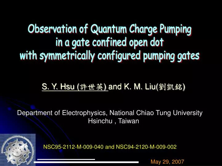
Observation of Quantum Charge Pumping in a gate confined open dot with symmetrically configured pumping gates. S. Y. Hsu ( 許世英 ) and K. M. Liu( 劉凱銘 ). Department of Electrophysics, National Chiao Tung University Hsinchu , Taiwan. NSC95-2112-M-009-040 and NSC94-2120-M-009-002.

E N D
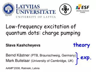
Observation of Quantum Charge Pumping in a gate confined open dot with symmetrically configured pumping gates S. Y. Hsu (許世英) and K. M. Liu(劉凱銘) Department of Electrophysics, National Chiao Tung University Hsinchu , Taiwan NSC95-2112-M-009-040 and NSC94-2120-M-009-002 May 29, 2007
I Pumping in a Quantum Device V(t) right reservoir left reservoir I Quantum system DC current left reservoir A coherent electron system e- Thouless pump : a traveling wave PRB 27, 6083 (1983) A phenomena when the dc current is generated in the system with the local perturbation only, without a global driving (bias).
Outline • Introduction • 2DEG • Gate-confined nanostructures • Historical review on charge pumping • Experimental results and discussion • Pumping and Rectification in our QD • Summary
0.2eV E1 2DEG Ec Ef energy Two Dimensional Electron Gas Structure of GaAs/AlGaAs grown by MBE The 2DEG systems are generally formed by GaAs/AlGaAs heterostructure and contain a thin conducting layer in the interface. 10 nm, GaAs Cap 8 nm, spacer AlGaAs 15 nm, δ- doping layer, Si, 2.6x1018 cm-2 60 nm, spacer AlGaAs x=0.37 1500 nm, buffer layer GaAs 2DEG specification 0.3mm GaAs substrate Our wafers were grown by Dr.Umansky in Heiblum’s group at Wiezmann Institute in Israel.
Photo-lithography E-beam lithography mesa 190m contact pads metal gates 0.5m
e- Source Drain Vg Gate confined nanostructures Applying negative voltages on the metal gates fabricated above a two dimensional electron gas(2DEG), a quasi-1D quantum conductor is formed. Three dimensional representation of V. For a parabolic confining potential kx Energy dispersion for 1D channel En (for n=1,2,3) vs. longitudinal wavevector kx. Electrons in the source and drain fill the available states up to chemical potentials s and d, respectively.
T=0.3K N 1D 2D Each plateau corresponds to an additional mode as integer multiples of half the Fermi wavelength Split gates confined QPC : dgap=0.3m and channel=0.5 m Two terminal Landauer formula N: integer
Quantum dots can be formed by placing two quantum point contacts in series in between source and drain and confining electrons in between to a small area characterized by F<L<. A coherent system
A QuantizedPumping in narrow channel usingSAWs Surface Acoustic Waves SAW generating transducer Split gate -Shilton et al., 2DEG J. Phys. C. 8, L531(1996), PRB62, 1564 (2000). I=nef, f=2.728GHz Pinched-off regime • Electrons reside in potential valleys and • are carried by the SAW. • Each plateau corresponds to a discrete number • of electrons in an electron packet.
Adiabatic Charge Pumping in a QD Brouwer (1998) Vac,1sin(t) For an open confined cavity with two parameters modifying wavefunction with a phase shift , use S-matrix and treat the ac field as a weak perturbation Vac,2sin(t+) emissivity The charge Q(m) entering or leaving the cavity through contact m(m=1,2) in an infinitesimal time: After Fourier Transform, integrating over one period and change of variables PRB 58, 10135 (1998).
Electron pumping in an open dot usingtwo RF signals Switkes et al., Science 283, 1905 (1999) Ibias=0 Vacsin(t) Vacsin(t+) V() sin() • σ(A0) f. slope~3pA/MHz (20 electrons/cycle) • For small driving amplitude, σ(A0) Vac2.
Adiabatic Quantum Charge Pumping or Rectification of Displacement Current ?
Rectification of displacement currents Brouwer, PRB63, 12130 (2001). The two ac gates coupled to the reservoir via stray capacitances C1 and C2. At low frequency, ac X1 and X2 generate displacement current through the dot. Average over one period, Equivalent circuit for the experiment of Switkes et al..
Experimental details qpc1 qpc2 Vg1 Vg2 The quantized conductance of each QPC is clearly present. Quantum dot is formed by placing two QPCs in series. We can adjust transmission mode number N=(n1, n2) for the “open” quantum dot. n1: mode number on the left QPC n2: mode number on the right QPC
FG 1m Vacsin(t+1) qpc1 qpc2 Vacsin(t+2) FG A Measurements : Low frequency modulation technique (1) Pumping mode (2) Rectification mode FG Vsdsin(t+1) 1m qpc1 qpc2 FG Vacsin(t+2) A A typical plot of I().
I I’=? How is the charge pumping influenced by by coupling with its environments ? Vac1sin(t) Vac1sin(t) reservoir reservoir wider Vac2sin(t+) Vac2sin(t+)
Experimental results DC current amplitude Ip & Irect vs. ac driving amplitude Vac DC current amplitude Ip& Irect vs. ac driving frequency f for different couplings between dot and its reservoir. (n1, n2).
Pumped current amplitude Ip vs. ac driving amplitude Vac Good resolution as small as few pA. • It’s in weak pumping regime. • IpVac2, in good agreement with the theoretical prediction. • The relation extends well over a very wide current range, • 3 orders in magnitude.
Rectification current amplitude Irect vs. Vac Consistent with the theoretical prediction.
Pumped current amplitude Ip vs. ac driving frequency f for different (n1, n2) Vac =15mV • Ip is roughly linearly dependent with frequency. • Ip is smaller for larger Ntot.
Rectification current amplitude Irec vs. ac driving frequency f for different (n1, n2) • Irect decreases with f for f1MHz and slightly increases with f for f>1MHz. • Irect increases with N (conductance), but saturates for Ntot4.
Dependence of Ip on the coupling bet. dot and its environments Comparing with (1,1) trace, multiply other traces with a factor (n1+n2)/2 Ip is scaling with the ratio between mode numbers.
With shorter dwell time, the coherent effect is reduced. Therefore, quantum pumping is suppressed w/. increasing Ntot. Why do n1 and n2 influence Ip? n1 and n2are transmission mode numbers of both “entrance” leads of the “open” dot, respectively. • For the larger mode number, electrons have stronger coupling strength between dot and reservoirs. The escaping rate of electron in the dot • The escaping rate esc increases with mode number linearly, and electrons are more likely to escape to the reservoirs.
The observed DC current in the pumping mode is mainly from the pumping effect. Summary The dc current characteristics of pumping and rectification effects are drastically different in our systems. The pumping current decreases with increasing transmission mode numbers of the two QPCs due to the dephasing of the coherent electrons in the dot by rapid motions of entering and leaving the dot. symmetric arrangement of pumping gates relative to both entrance leads of the dot
Thanks for your attention ! Acknowledgments: Dr. C.S. Chu (Theoretical support) Dr. V.Umansky (High mobility 2DEG support)