Download

1 / 94
1.01k likes | 1.12k Views
Microprocessor and interfacing techniques. 1. Prerequisites: Microprocessor Architecture Course Objectives: 1. To learn the Peripheral architecture and programming 0f Microprocessor. 2. To learn peripherals and their interfacing with 8086 Microprocessor. 3. To study the DOS Internals.

E N D
Prerequisites: Microprocessor Architecture • Course Objectives: 1. To learn the Peripheral architecture and programming 0f Microprocessor. 2. To learn peripherals and their interfacing with 8086 Microprocessor. 3. To study the DOS Internals. 4. To Study NDP and Design of Microprocessor based System. • Course Outcomes: 1.Ability to handle, interface and program using legacy peripherals 2.Ability to understand I/O Hub functions 2
Books • 80386 – Tata Mcgraw Hill – Turley • Adv microprocessors and peripherals - Tata Mcgraw Hill – Ray • Microprocessors and interfacing – McGraw – Douglas Hall • Advanced MS DOS programming – Ray Duncan • Assembly language programming – Pearson – Peter Abel 3
Bits and bytes • 1 Bit = Binary Digit • 8 Bits = 1 Byte • 1024 Bytes = 1 Kilobyte • 1024 Kilobytes = 1 Megabyte • 1024 Megabytes = 1 Gigabyte • 1024 Gigabytes = 1 Terabyte • 1024 Terabytes = 1 Petabyte • 1024 Petabytes = 1 Exabyte • 1024 Exabytes = 1 Zettabyte • 1024 Zettabytes = 1 Yottabyte • 1024 Yottabytes = 1 Brontobyte • 1024 Brontobytes = 1 Geopbyte 4
What is a microprocessor? • An integrated circuit that performs the functions of a CPU. • So, a chip on machine… • Which microprocessors do you know? • 8085,8086,80285,80386,486,pentium….. • Which is latest? • Intel core i3, i5, i7 • What type of processor? • 16 or 32 or 64? 5
32 or 64 bit? • What determines that my machine is 32 or 64? • Amount of data that can be handled • The RAM support for 32 bit is 4 GB where as for 64 it is 16EB. • 64 bit of course leads to faster operations. 6
What is 8086? • It is a 16 bit µp. • 8086 has a 20 bit address bus can access up to 220 memory locations ( 1 MB) . • It can support upto 64K I/O ports. • It provides 14, 16-bit registers. • It has multiplexed address and data bus AD0- AD15 and A16 – A19. 7
Architecture of 8086 • 8086 has two blocks BIU and EU. • The BIU performs all bus operations such as instruction fetching, reading and writing operands for memory and calculating the addresses of the memory operands. • The instruction bytes are transferred to the instruction queue. • EU executes instructions from the instruction system byte queue. 9
Architecture of 8086 ctd… • BIU and EU operate asynchronously to give the 8086 an overlapping instruction fetch and execution mechanism which is called as Pipelining. • This results in efficient use of the system bus and system performance. • BIU contains Instruction queue, Segment registers, Instruction pointer, Address adder. • EU contains Control circuit, Instruction decoder, ALU, Pointer and Index register, Flag register 10
Architecture of 8086 ctd… • Bus Interface Unit: • It provides a full 16 bit bidirectional data bus and 20 bit address bus. • The bus interface unit is responsible for performing all external bus operations. • Specifically it has the following functions: • Instruction fetch, Instruction queuing, Operand fetch and storage, Address relocation and Bus control. • The BIU uses a mechanism known as an instruction stream queue to implement a pipeline architecture. 11
Architecture of 8086 ctd… • EXECUTION UNIT : • The Execution unit is responsible for decoding and executing all instructions. • The EU extracts instructions from the top of the queue in the BIU, decodes them, generates operands if necessary, passes them to the BIU and requests it to perform the read or write bys cycles to memory or I/O and perform the operation specified by the instruction on the operands. • During the execution of the instruction, the EU tests the status and control flags and updates them based on the results of executing the instruction. 12
Important Pin descriptions • AD0-Ad15: Multiplexed memory/IO address and data bus. • ALE: High the lower order bits to be latched, then these can be used for the data. • READY: Acknowledgement from addressed memory or IO that it will complete the operation. • INTR: Level triggered input, helps in determining whether the processors should enter into interrupt ack operation. A subroutine is vectored through an interrupt vector table. • INTA: interrupt ack from the Microprocessor • RESET: Causes processor to terminate its present activity. Signal must be high fro atleast 4 clock cycles. Restarts the execution. 14
Pin descriptions • AD0-Ad15: Multiplexed memory/IO address and data bus. • ALE: High the lower order bits to be latched, then these can be used for the data. • READY: Acknowledgement from addressed memory or IO that it will complete the operation. • INTR: Level triggered input, helps in determining whether the processors should enter into interrupt ack operation. A subroutine is vectored through an interrupt vector table. • INTA: interrupt ack from the Microprocessor • RESET: Causes processor to terminate its present activity. Signal must be high fro atleast 4 clock cycles. Restarts the execution. 15
The Programming Model 8086 • General Purpose Registers • Segment Registers • Flag Register • Pointer and index Registers SP BP AH AX AL CS SI BX DS BL BH DI CX ES CH CL IP DX DH DL SS Flag Flag Register General Purpose Segment Registers Pointer and Index Registers 17
Registers Organisation • 16-Bit General Purpose Registers – can access all 16-bits at once – can access just high (H) byte, or low (L) byte only the General Purpose registers allow access as 8-bit High/Low sub-registers 18
Registers Organisation (continued) • Register Set 16-Bit Segment Addressing Registers CS Code Segment DS Data Segment SS Stack Segment ES Extra Segment 19
Registers Organisation (continued) 16-Bit Offset Addressing Registers SP Stack Pointer BP Base Pointer SI Source Index DI Destination Index 20
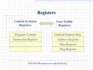
Registers Organisation (continued) 16-Bit Control/Status Registers - IP Instruction Pointer (Program Counter for execution control) - FLAGS 16-bit register • It is not a 16-bit value but it is a collection of 9 bit-flags (six are unused) • Flag is set when it is equal to 1 • Flag is clear when it is equal to 0 21
General purpose Registers • AX • Accumulator Register • Preferred register to use in arithmetic, logic and data transfer instructions because it generates the shortest Machine Language Code • Must be used in multiplication and division operations • Must also be used in I/O operations 22
General purpose Registers (conti..) • BX • Base Register • Also serves as an address register • Used in array operations 23
General purpose Registers (conti..) • CX • Count register • Used as a loop counter • Used in shift and rotate operations • DX • Data register • Used in multiplication and division • Also used in I/O operations 24
Pointer & Index Registers • Contain the offset addresses of memory locations • Can also be used in arithmetic and other operations • SP: Stack pointer • Used with SS to access the stack segment 25
Pointer & Index Registers (continued) • BP: Base Pointer • Primarily used to access data on the stack • Can be used to access data in other segments • SI: Source Index register • is required for some string operations • When string operations are performed, the SI register points to memory locations in the data segment which is addressed by the DS register. Thus, SI is associated with the DS in string operations. 26
Pointer & Index Registers (continued) • DI: Destination Index register • is also required for some string operations. • When string operations are performed, the DI register points to memory locations in the data segment which is addressed by the ES register. Thus, DI is associated with the ES in string operations. • The SI and the DI registers may also be used to access data stored in arrays 27
Segment Registers • Are Address registers • Store the memory addresses of instructions and data • Memory Organization • Each byte in memory has a 20 bit address starting with 0 to 220-1 of addressable memory 28
Segment Registers (continued) • Addresses are expressed as 5 hex digits from 00000 - FFFFF • Problem: But 20 bit addresses are TOO BIG to fit in 16 bit registers! • Solution: Memory Segment • Block of 64K (65,536) consecutive memory bytes • A segment number is a 16 bit number 29
Segment Registers (continued) • Segment numbers range from 0000 to FFFF • Within a segment, a particular memory location is specified with an offset • An offset also ranges from 0000 to FFFF 30
Segment Registers (continued) • If the segment address is for example, 2915, then the addresses in this segment start at 2915:0000 and go up to 2915:FFFF, which is the highest address in this particular segment. • This range expressed in terms of absolute or physical addresses is from 29150 through 3914F. The relationship between a segment and the register which defines it is shown below. 31
Segment Registers (continued) 32 Memory Model for 20-bit Address Space
Memory Address Generation Offset Value (16 bits) 0 0 0 0 Segment Register (16 bits) Adder Physical Address (20 Bits) 35
Memory Address Generation • to calculate physical memory address 36
Flag Register Carry flag Overflow Parity flag Direction Interrupt enable Auxiliary flag Trap Zero Sign 6 are status flags 3 are control flag 37
Power Supply 5V 10% Ground Reset Registers, seg regs, flags CS: FFFFH, IP: 0000H If high for minimum 4 clks Clock Duty cycle: 33% Minimum mode operation 39
Minimum mode operation ( Conti..) Address/Data Bus: Contains address bits A15-A0 when ALE is 1 & data bits D15 – D0 when ALE is 0. Address Latch Enable: When high, multiplexed address/data bus contains address information. 40
Minimum mode operation ( Conti..) Non-maskable interrupt Interrupt acknowledge Interrupt request INTERRUPT 41
Minimum mode operation ( Conti..) Hold Hold acknowledge Memory Access 42
Minimum mode operation ( Conti..) S6: Logic 0. S5: Indicates condition of IF flag bits. S4-S3: Indicate which segment is accessed during current bus cycle: Address/Status Bus Address bits A19 – A16 & Status bits S6 – S3 43
Bus High Enable/S7 Enables most significant data bits D15 – D8 during read or write operation. S7: Always 1. Minimum mode operation ( Conti..) BHE#, A0: 0, 0: Whole word (16-bits) 0,1: High byte to/from odd address 1,0: Low byte to/from even address 1,1: No selection 44
Min/Max mode Minimum Mode: +5V Maximum Mode: 0V Min mode pins Minimum mode operation ( Conti..) 45
When 1, transmit mode, when 0 receive mode from memory or IO Determined by wait instruction, when goes low, continue else idle state Minimum mode operation ( Conti..) Indicates the availability of valid data over address and data lines. Active from t2 to t4 46
Minimum mode operation ( Conti..) Read Signal Write Signal Memory or I/0 Data Bus Enable 47
Maximum mode operation ( Conti..) Status Signal Inputs to 8288 to generate eliminated signals due to max mode. S2 S1 S0 000: INTA 001: read I/O port 010: write I/O port 011: halt 100: code access 101: read memory 110: write memory 111: none -passive 50