Download
1 / 20
240 likes | 561 Views
Ion Implantation and Ion Beam Analysis of Silicon Carbide Zsolt Z OLNAI MTA MFA Research Institute for Technical Physics and Materials Science Budapest, Hungary. University of Hyderabad 4 th October 2007. Outline • SiC: physical properties and applications

E N D
Ion Implantation and Ion Beam Analysis of Silicon Carbide Zsolt ZOLNAI MTA MFA Research Institute for Technical Physics and Materials Science Budapest, Hungary University of Hyderabad 4th October 2007
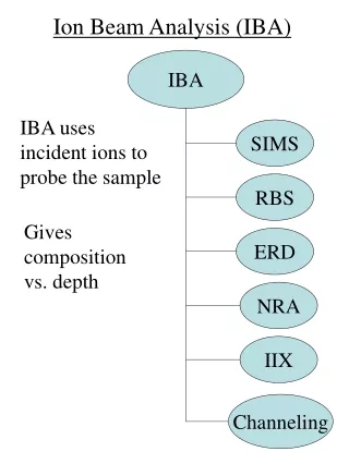
Outline • SiC: physical properties and applications • 3.5 MeV 4He+ion backscattering spectrometry in combination with channeling (BS/C) • He+ implantation into SiC • N+ implantation into SiC from channeling direction • High dose Ni+ implantation into SiC
SiC: applications Semiconductor technology Infineon: Schottky diodes CREE: 4H, 6H-SiC substrates SiC Space applications Nuclear Energetics ESA: ultra-light weight mirrors ITER: first wall material Other: spintronics, optoelectronics, etc.
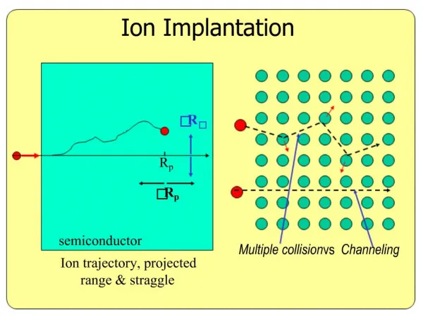
SiC technology: selectivedoping p - type (Al, Ga, B) SiC n - type (N, P) Slow diffusion of dopants (below 2000 oC) Selective doping byionimplantation Generation of Crystal Defects (vacancies, antisites, interstitials, extended defects, complexes) Modification of the electrical properties (Carrier trapping, detrapping) 10-100 keV
(1120) A C C C A site <0001> B B B B B site <1100> C site A A A A SiC: polytypes C atom Si atom c-axis 6H-SiC 4H-SiC 3C-SiC 2H-SiC
3.5 MeV 4He+Ion Backscattering Analysison SiC 4He+ = 165o Favourable for Si and C sulattice studies!
The damaging effect of the analyzing He+ ion beam saturation N. Q. Khánh et al., Nucl. Instrum. Methods Phys. Res. B 161-163 (2000) pp 424-428
Electronic stopping power for channeled He+ions along the [0001] axis of 6H-SiC: application in BS/C spectrum analysis SeChannel = SeRandom Crystal-TRIM simulation: = 0.8 Damage distributions in N+ implanted SiC (No thermal diffusion of defects expected) BS/C spectrum analysis
Implantation of 500 keV N+ ions into 6H SiC: the influence of channeling on damage production N+ Beam tilting Beam tilt angles: 0o, 0.5o, 1.2o, 1.6o, 4o Critical angle for channeling CRIT = 1.7o 0001 axis 6H-SiC
Implantation of 500 keV N+ ions into 6H SiC: the influence of channeling on damage production Tilt angles with respect to the [0001] axis: 0o, 0.5o, 1.2o, 1.6o, 4o 3.55 MeV 4He+ BS/C spectra RBX simulation of BS/C spectra
Implantation of 500 keV N+ ions into 6H SiC: the influence of channeling in damage production 0001 axis N+ Reduccd damage for channeling No surface defects: good for the determination of the parameter for He 0001 axis N+ Z. Zolnai et al., J. Appl. Phys. 101 (2007) 023502
Implantation of 500 keV N+ ions into 6H SiC: the influence of channeling in damage production Crystal-TRIM simulation for 500 keV N+ implant: SiC BS/C spectrum analysis Z. Zolnai et al., j. Appl. Phys. 101 (2007) 023502
Implantation of 500 keV N+ ions into 6H SiC: the influence of channeling in damage production 0001 axis Dose dependence of damage N+
Implantation of 500 keV N+ ions into 6H SiC: the influence of channeling in damage production Direct-impact, defect-stimulated (D-I/D-S) amorphization model S = fa + Sd = 1 − g(D) + Sdmax[1 − exp(− BD)]g(D) S: total disorder fa : amorphization in collision cascades Sd: point defect generation and g(D) = (a + s)/ (s + a exp [{a + s}D]) a : direct impact amorphization cross-section s : defect stimulated amorphization cross-section Z. Zolnai et al., J. Appl. Phys. 101 (2007) 023502
Implantation of 500 keV N+ ions into 6H SiC: the influence of channeling in damage production 500 keV N+: SiC 3.5 MeV He+: SiC High-energy light ions: The direct impact amorphization is negligible! (dilute collision cascasdes)
Diluted magnetic semiconductors: doping by transition metal ions (Fe, Co, Ni, Mn, Cr, V, etc.) for spintronics applications Wide bandgap semiconductor high Curie temperature! Doping with Mn, Fe, Co, Ni, Cr, V, etc Carrier mediated ferromagnetism Tested in GaAs, ZnO, GaN, ... SiC is a possible candidate (bandgap is 3.26 eV for 4H polytype)
High dose 860 keV Ni+ implantation into 4H-SiC 1x10¹⁶/cm2 (0001) SiC 3x10¹⁶/cm2 (0001) SiC 5x10¹⁶/cm2 (0001) SiC 1x10¹⁶/cm2 (11-20) SiC 1150 oC annealing, 1 h, in Ar atm.
High dose Ni+ implantation into 4H-SiC 860 keV Ni implantation, 1x10¹⁶/cm2 1150 oC annealing, 1 h, in Ar atm. 4H-SiC (11-20) 4H-SiC (0001)