Download
1 / 23
270 likes | 655 Views

E N D
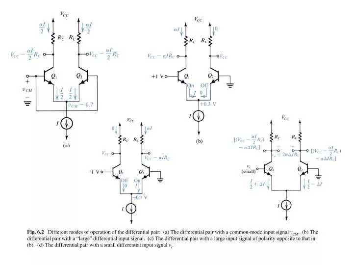
Fig. 6.2 Different modes of operation of the differential pair: (a) The differential pair with a common-mode input signal vCM. (b) The differential pair with a “large” differential input signal. (c) The differential pair with a large input signal of polarity opposite to that in (b). (d) The differential pair with a small differential input signal vi.
Fig. 6.3 Transfer characteristics of the BJT differential pair of Fig. 6.2 = 1 assuming 1.
Fig. 6.4 The current an voltages in the differential amplifier when a small difference signal vdis applied.
Fig. 6.5 A simple technique for determining the signal currents in a differential amplifier excited by a differential voltage signal vd; dc quantities are not shown.
Fig. 6.6 A differential amplifier with emitter existence. Only signal quantities are shown (on color).
Fig. 6.7 Equivalence of the differential amplifier (a) to the two common-emitter amplifiers in (b). This equivalence applies only for differential input signals. Either of the two common-emitter amplifiers in (b) can be used to evaluate the differential gain, input differential resistance, frequency response, and so on, of the differential amplifier.
Fig. 6.10 (a) The differential amplifier fed by a common-mode voltage signal. (b) Equivalent “half-circuits” for the common-mode calculations.
Fig. 6.16 Analysis of the current mirror taking into account the finite of the BJTs.
Fig. 6.26 Small-signal model of the differential amplifier of Fig. 6.25.
Fig. 6.27 (a) The differential form of the cascode amplifier, and (b) its differential half circuit.
Fig. 6.28 A cascode differential amplifier with a Wilson current-mirror active load.
Fig. 6.30 Normalized plots of the currents in a MOSFET differential pair. Note that VGSis the gate-to-source voltage when the drain current is equal to the dc bias current (I/2).
Fig. 6.32 MOS current mirrors: (a) basic, (b) cascode, (c) Wilson, (d) modified Wilson.
Fig. 6.35 basic active-loaded amplifier stages; (a) bipolar; (b) MOS; (c) BiCMOS obtained by cascoding Q1 with a BJT, Q2; (d) BiCMOS double cascode.
Fig. 6.36 Voltage gain of the active-loaded common-source amplifier versus the bias current ID. Outside the subthreshold region, this is a plot of Eq. (6.121) for the casenCox = 20 A/V2, = 0.05 V-1, L = 2 m and W = 20 m.