Download
1 / 11
110 likes | 195 Views
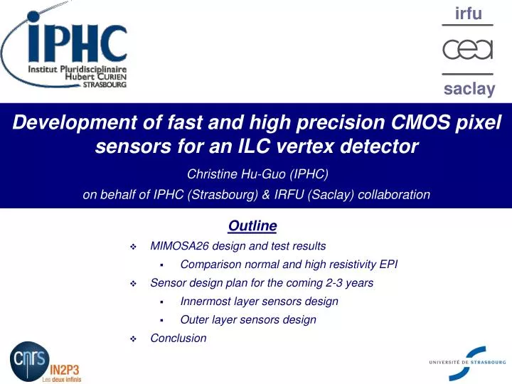
Development of fast and high precision CMOS pixel sensors for an ILC vertex detector Christine Hu-Guo (IPHC) on behalf of IPHC (Strasbourg) & IRFU (Saclay) collaboration. Outline MIMOSA26 design and test results Comparison normal and high resistivity EPI

E N D
Development of fast and high precision CMOS pixel sensors for an ILC vertex detectorChristine Hu-Guo (IPHC)on behalf of IPHC (Strasbourg) & IRFU (Saclay) collaboration Outline • MIMOSA26 design and test results • Comparison normal and high resistivity EPI • Sensor design plan for the coming 2-3 years • Innermost layer sensors design • Outer layer sensors design • Conclusion
MIMOSA26 Active area: ~10.6 x 21.2 mm2 13.7 mm 0.64 mV 0.31 mV 21.5 mm Development of CMOS Pixel Sensors for Charged Particle Tracking • 2009, an important year for CMOS pixel sensors R&D: MIMOSA26 has been designed, fabricated and tested within the EUDET program • MIMOSA26 is a reticule size MAPS with binary output, 10 k images / s • Pixel array: 1152 x 576, 18.4 µm pitch • Architecture: • Pixel (Amp+CDS) array organised in // columns r.o.in the rolling shutter mode • 1152 ADC, a 1-bit ADC (discriminator) / column • Integrated zero suppression logic • Remote and programmable • Lab. and beam tests: 62 chips tested, yield ~75% Efficiency 99.5% for fake rate 10-4 ENC ~ 13-14 e- Single point resolution ~4 µm IRFU - IPHC christine.hu@ires.in2p3.fr
MIMOSA26 Test • Standard EPI layer (fab. end 2008) v.s. high resistivity EPI layer (fab. end 2009) • Charge collection & S/N (Analogue output, Freq. 20 MHz) • Radiation test under way for applications more demanding than ILC • Ionising TID: 150 K , 300 K, 1M Rad • Non Ionising NIEL: 3x10¹², 6x10¹², 1x10¹³, 3x10¹³ Neq/cm2 • MIMOSA26 can be operated at a high readout speed • Clock frequency: from 80 MHztyp. (~110 µs) up to 110 MHz (~80 µs) • MIMOSA26: design base line for STAR Vx upgrade, CBM MVD Its performances are close to the ILD vertex detector specifications IRFU - IPHC christine.hu@ires.in2p3.fr
ILD design: 2 options 3 double layers 5 single layers ILC VTX: R&D of CMOS Sensors • Innermost layer sensors: • tint. ~ 25 μssp < 3 μm R&D effort on high readout speed design • Double-sided readout (for both design options) • Elongated pixels (for 3 double layers option: time stamp tier) • Outer layer sensors: • tint. <~ 100 μs sp ~ 3-4 μm R&D effort on low power consumption design • Single-sided readout (for both design options) • 4-bit column-level ADCs • Power consumption: • Pdiss < 0.1–1 W/cm² ( ×~ 1/50 duty cycle ) IRFU - IPHC christine.hu@ires.in2p3.fr
Matrix for time stamp Matrix for resolution Sensors for resolution Flex cable Foam Support Flex cable Sensors for time stamp Innermost Layer CMOS Sensor's Development • 1st R&D line: double-sided readout • Based on architecture of MIMOSA26 • Rolling shutter readout mode + A/D conversion binary output + zero suppression • Pixel array: ~ 14 µm pitch • Active area: ~ 9 x (~ 20) mm² • tint. <~ 40-60 µs • Pdiss <~ 1 W/cm² ( × ~ 1/50 duty cycle) • 2ndR&D line: elongated pixels • Time stamp tier for 3 double layers option • Ex: 14 x (4 x 14 µm) • tint. <~ 10-15 µs • High resistivity EPI process useful • High charge collection efficiency Elongated pixel "Plume"Project Integration topic Collaboration:Strasbourg, DESY, Oxford, Bristol, ... See Nathalie Chon-Sen's talk: IRFU - IPHC christine.hu@ires.in2p3.fr
Pixel Array Column-level ADC Controller+Memory+DAC+Trans. ILC Outer layer CMOS Sensor's Development • Large pitch pixels associated with column-level ADC power consumption reduction • Single-sided readout • Pixel array: 576 x 576, pitch 35 µm • 4-bits ADC / column • tint. ~ 60 - 100 µs • Pdiss <~ 0.2 W/cm² ( x ~ 1/50 duty cycle ) • Different column-level ADC architectures have been investigated in IN2P3-CEA collaboration • Taking integration experience of MIMOSA26, ADC's architecture will be extended to several hundreds ADCs converting all signals of a row simultaneously • Noise from substrate coupling • Coupling between ADC • Long common reference line (~2 cm) for whole chip • Offset compensation • Clock and control signals management Submission of a small sensor but a sizable prototype: pixel array + column-level ADC IRFU - IPHC christine.hu@ires.in2p3.fr
MIMOSA27 Exploration of new process • Using a smaller feature size CMOS technology: 0.18 µm • High speed operation inside chip • Surface reduction in digital design • Reduce power consumption … • Offer more metal layers for interconnection decrease dead zone • MIMOSA27 in a 0.18 µm process (up to 6 metal layers) will be submitted on April 9th, 2010 • 10 mm², 20 µm pitch, 4 sub-matrices of 64 x 64 • Up to16 options: • Diode size and type of configuration • 3 T and self-bias • In pixel amplification • Study: • Charge collection efficiency • Technology features • Signal to noise ratio • Radiation hardness • … IRFU - IPHC christine.hu@ires.in2p3.fr
digital process (number of metal layers)feature size fast laser driver, etc. Digital Analog ~ 50 µm Sensor Using 3DIT to improve MAPS performances (1) • 3DIT are expected to be particularly beneficial for MAPS : • Combine different fabrication processes Split signal collection and processing functionalities use best suited technology for each Tier : • Tier-1: charge collection system Epitaxy (depleted or not) ultra thin layer X0 • Tier-2: analogue & mixed signal processing analogue, low Ileak, process (No. of metal layers) • Tier-3: digital signal processing & data transmission • (Tier-4: data transmission, electro-optical conversion ?) • Resorb most limitations specific to 2D MAPS • Dead surface • Power consumption • Readout speed • … • 2009: run in Chartered - Tezzaron technology • 3D consortium: coordinated by FermiLab • 130 nm, 2-Tier run with "high"-res substrate (allows m.i.p. detection) • Tier A to tier B bond Cu-Cu bond IRFU - IPHC christine.hu@ires.in2p3.fr
Tier 1 Tier 2 Acquisition Readout A B Detection diode or Q injection Amplifier Amp.+Shaper Discriminator Hit identification 5 bits (7?) Time Stamp 2nd hit flag ReadOut ~1 ms + ~200 ms ~1 ms 24 µm TS & R.O. ASD 12 µm 12 µm Detection diode & Amp Using 3DIT to improve MAPS performances (2) • Delayed R.O. Architecture for the ILC Vertex Detector (designed & submitted) • Try 3D architecture based on small pixel pitch, motivated by : • Single point resolution < 3 μm with binary output • Probability of > 1 hit per train per pixel << 10 % • 12 μm pitch : • sp ~ 2.5 μm • Probability of > 1 hit/train/pixel < 5 % • 3D 2-tier process • Tier-1: A: sensing diode & amplifier, B: shaper & discriminator • Tier-2: time stamp (5 bits) + overflow bit & delayed readout Architecture prepares for 3-Tier perspectives : 12 µm • Tier-1: CMOS process adapted to charge collection • Tier-2: CMOS process adapted to analogue & mixed signal processing • Tier-3: digital process (<< 100 nm ?) IRFU - IPHC christine.hu@ires.in2p3.fr
RO Sparsification 4-bit ADC Detection diode & Amplifier ~18-20 µm Using 3DIT to improve MAPS performances (3) • MAPS with fast pipeline digital readoutaiming to minimise power consumption (R&D in progress) • Subdivide sensitive area in ”small” matrices running individually in rolling shutter mode • Adapt the number of raws to required frame readout time few µs r.o. time may be reached • Design in 20 µm²: • Tier 1: Sensor & preamplifier (G ~ 500 µV/e-) • Tier 2: 4-bit pixel-level ADC with offset cancellation circuitry (LSB ~ N) • Tier 3: Fast pipeline readout with data sparsification sp ~ 2 μmTint. < 10 µs IRFU - IPHC christine.hu@ires.in2p3.fr
Conclusion • MIMOSA26's performances are close to ILD vertex detector specifications • Architecture will evolve to meet VTX performances • Innermost layer: double sided readout readout speed trade-off • Outer layer: matrix + column-level ADC power consumption trade-off • Fabrication processes with high resistivity EPI layer will improve read-out speed and radiation tolerance • Time stamp layer • Integration of column-level ADCs with pixel array in progress Prototyping of inner and outer layer sensors expected to be nearly finalised by 2012 for ILD-DBD • Translation to 3DIT will resorb most limitations specific to 2D MAPS • Still many difficulties to overcome • Offer an improved read-out speed : O(μs) + Lower power consumption IRFU - IPHC christine.hu@ires.in2p3.fr