Download
1 / 38
420 likes | 698 Views
บทที่ 2 Semiconductor and P-N junction. Semiconductor material. Silicon wafer. Semiconductor material. Silicon crystal. Sand 25% silicon. Semiconductor material. Silicon atom. Intrinsic semiconductor. Silicon Crystal at T= 0 °K. Energy gap. Energy level.

E N D
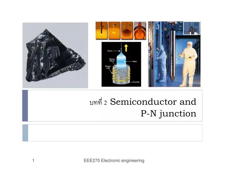
บทที่ 2 Semiconductor and P-N junction EEE270 Electronic engineering
Semiconductor material Silicon wafer EEE270 Electronic engineering
Semiconductor material Silicon crystal Sand 25% silicon EEE270 Electronic engineering
Semiconductor material EEE270 Electronic engineering
Silicon atom EEE270 Electronic engineering
Intrinsic semiconductor Silicon Crystal at T= 0 °K EEE270 Electronic engineering
Energy gap EEE270 Electronic engineering
Energy level An electron-volt is the energy of an electron that has been accelerated through a potential difference of 1 volt, and 1eV= 1.6*10-19 joules EEE270 Electronic engineering
Intrinsic semiconductor Silicon Crystal at T > 0 °K EEE270 Electronic engineering
The Intrinsic Carrier Concentration ni is the intrinsic carrier concentration B is a constant related to the specific semiconductor material Eg is the band-gap energy (eV) T is the temperature (°K) k is Boltzmann’s constant (86 x 10-6eV/°K) EEE270 Electronic engineering
Electrical current EEE270 Electronic engineering
Doping and Extrinsic Semiconductors EEE270 Electronic engineering
Basic silicon doping ขั้นตอนในการแพร่สารเจือเบื้องต้น หลักการแพร่กระจายของหมึกในนํ้า แสดงการแพร่สารเจือ (Diffusion) เกิดเป็นรอยต่อ P-N EEE270 Electronic engineering
Type of doping process เตาแพร่สารเจือที่มีแหล่งจ่ายเป็นของแข็ง เตาแพร่สารเจือที่มีแหล่งจ่ายเป็นของเหลว เตาแพร่สารเจือที่มีแหล่งจ่ายเป็นแก๊ส การโดปโดยใช้วิธียิงอิออน (Ion-Implantation) EEE270 Electronic engineering
N-type semiconductor EEE270 Electronic engineering
P-type semiconductor EEE270 Electronic engineering
Thermal equilibrium no = thermal equilibrium concentration of free electron po = thermal equilibrium concentration of hole Silicon Crystal at T > 0 °K EEE270 Electronic engineering
Thermal equilibrium (N-type) EEE270 Electronic engineering
Thermal equilibrium (P-type) EEE270 Electronic engineering
Drift and Diffusion Currents EEE270 Electronic engineering
Drift and Diffusion Currents EEE270 Electronic engineering
Drift and Diffusion Currents EEE270 Electronic engineering
Drift and Diffusion Currents EEE270 Electronic engineering
Drift and Diffusion Currents EEE270 Electronic engineering
Drift and Diffusion Currents EEE270 Electronic engineering
Drift and Diffusion Currents EEE270 Electronic engineering
Drift and Diffusion Currents EEE270 Electronic engineering
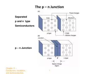
P-N junction Bell Labs the firsttransistor in December 1947. EEE270 Electronic engineering
P-N Junction EEE270 Electronic engineering
The Equilibrium P-N Junction EEE270 Electronic engineering
Barrier potential or Built-in voltage is called thermal voltage, approximately 0.026V at room temperature, T=300 °K The Equilibrium P-N Junction EEE270 Electronic engineering
Built-in voltage EEE270 Electronic engineering
P-N Junction biasing Forward-bias Non-bias Reward-bias EEE270 Electronic engineering
P-N Junction biasing EEE270 Electronic engineering
Junction capacitance EEE270 Electronic engineering
Reverse-Biased P-N Junction Reward-bias Cj : Junction Capacitance Cj0 : Junction Capacitance at zero applied voltage VR : Reverse bias voltage Vbi : built-in voltage EEE270 Electronic engineering
Forward-Biased P-N Junction Forward-bias IS : Reverse-bias Saturation current, in the range of 10-15 to 10-13 VT : Thermal voltage n : emission coefficient or ideality factor, in the range 1 n 2 EEE270 Electronic engineering
Forward-Biased P-N Junction EEE270 Electronic engineering