Download

1 / 9
90 likes | 305 Views
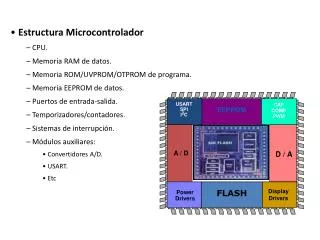
MICROCONTROLADOR. PIC 16F877. CPU RISC ARQUITECTURA HARVARD 35 INSTRUCCIONES DE ENSAMBLADOR EJECUCION EN 1 CICLO MÁQUINA MÁXIMA VEL 20MHZ. MEM PROGRAMA 8K-PALABRAS (FLASH) 368 KB MEM RAM DE DATOS 256 KB MEM EEPROM DE DATOS. CARACTERISTICAS (I). 1 WATCHDOG 3 TIMERS (8,16,8bits)

E N D
MICROCONTROLADOR PIC 16F877
CPU RISC ARQUITECTURA HARVARD 35 INSTRUCCIONES DE ENSAMBLADOR EJECUCION EN 1 CICLO MÁQUINA MÁXIMA VEL 20MHZ MEM PROGRAMA 8K-PALABRAS (FLASH) 368 KB MEM RAM DE DATOS 256 KB MEM EEPROM DE DATOS CARACTERISTICAS (I)
1 WATCHDOG 3 TIMERS (8,16,8bits) 2 CANALES PWM 8 CONVER. A/D de 10bits PUERTOS SERIE: SPI IIC USART PUERTO PARALELO ESCLAVO DE 8 BITS 33 PINES E/S EN 5 PUERTOS PILA HARWARE DEBUGGER IN CIRCUIT CARACTERISTICAS (II)
PUERTO A • Puerto de e/s de 6 pines • RA0 è RA0 y AN0 • RA1 è RA1 y AN1 • RA2 è RA2, AN2 y Vref- • RA3 è RA3, AN3 y Vref+ • RA4 è RA4 (Salida en colector abierto) y T0CKI(Entrada de reloj del modulo Timer0) • RA5 è RA5, AN4 y SS (Selección esclavo para el puerto serie síncrono)
PUERTO B • Puerto e/s 8 pines • Resistencias pull-up programables • RB0 è Interrupción externa • RB4-7 èInterrupcion por cambio de flanco • RB5-RB7 y RB3 è programacion y debugger in circuit
PUERTO C • Puerto e/s de 8 pines • RC0 è RC0, T1OSO (Timer1 salida oscilador) y T1CKI (Entrada de reloj del modulo Timer1). • RC1-RC2 è PWM/COMP/CAPT • RC1 è T1OSI (entrada osc timer1) • RC3-4 è IIC • RC3-5 è SPI • RC6-7 è USART
PUERTO D • Puerto e/s de 8 pines • Bus de datos en PPS (Puerto paralelo esclavo)
PUERTO E • Puerto de e/s de 3 pines • RE0è RE0 y AN5 y Read de PPS • RE1è RE1 y AN6 y Write de PPS • RE2è RE2 y AN7 y CS de PPS
REGISTROS DE DIRECCION • Confuguran si un pin es de entrada o de salida. • Se denominan: • TRISA • TRISB • ... • 0 significa Output (salida) • 1 significa Inpu (entrada)