Download
1 / 44
440 likes | 608 Views
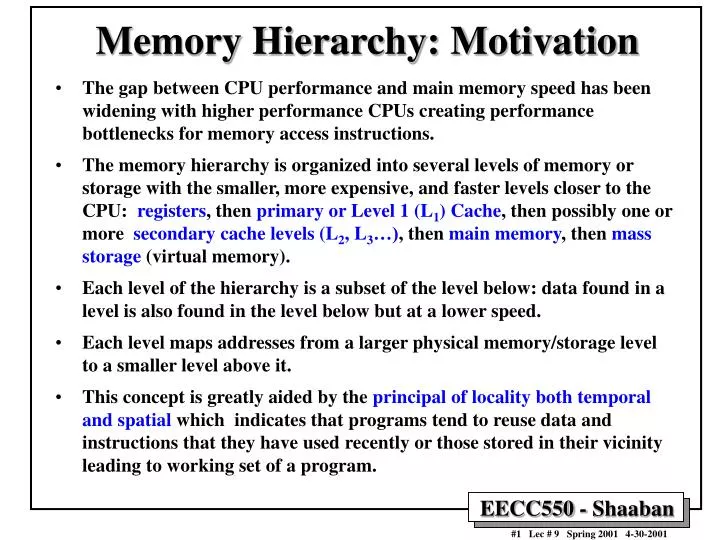
Memory Hierarchy: Motivation. The gap between CPU performance and main memory speed has been widening with higher performance CPUs creating performance bottlenecks for memory access instructions.

E N D
Memory Hierarchy: Motivation • The gap between CPU performance and main memory speed has been widening with higher performance CPUs creating performance bottlenecks for memory access instructions. • The memory hierarchy is organized into several levels of memory or storage with the smaller, more expensive, and faster levels closer to the CPU: registers, then primary or Level 1 (L1) Cache, then possibly one or more secondary cache levels (L2, L3…), then main memory, then mass storage (virtual memory). • Each level of the hierarchy is a subset of the level below: data found in a level is also found in the level below but at a lower speed. • Each level maps addresses from a larger physical memory/storage level to a smaller level above it. • This concept is greatly aided by the principal of locality both temporal and spatial which indicates that programs tend to reuse data and instructions that they have used recently or those stored in their vicinity leading to working set of a program.
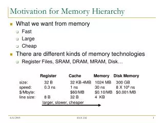
From Recent Technology Trends Capacity Speed (latency) Logic: 2x in 3 years 2x in 3 years DRAM: 4x in 3 years 2x in 10 years Disk: 4x in 3 years 2x in 10 years DRAM Year Size Cycle Time 1980 64 Kb 250 ns 1983 256 Kb 220 ns 1986 1 Mb 190 ns 1989 4 Mb 165 ns 1992 16 Mb 145 ns 1995 64 Mb 120 ns 1000:1 2:1
µProc 60%/yr. 1000 CPU 100 Processor-Memory Performance Gap:(grows 50% / year) Performance 10 DRAM 7%/yr. DRAM 1 1980 1981 1982 1983 1984 1985 1986 1987 1988 1989 1990 1991 1992 1993 1994 1995 1996 1997 1998 1999 2000 Memory Hierarchy: MotivationProcessor-Memory (DRAM) Performance Gap
Processor-DRAM Performance Gap Impact: Example • To illustrate the performance impact, assume a pipelined RISC CPU with CPI = 1 using non-ideal memory. • Over an 10 year period, ignoring other factors, the cost of a full memory access in terms of number of wasted instructions: CPU CPU Memory Minimum CPU cycles or Year speed cycle Access instructions wasted MHZ ns ns 1986: 8 125 190 190/125 = 1.5 1988: 33 30 175 175/30 = 5.8 1991: 75 13.3 155 155/13.3 = 11.65 1994: 200 5 130 130/5 = 26 1996: 300 3.33 100 110/3.33 = 33
Memory Hierarchy: MotivationThe Principle Of Locality • Programs usually access a relatively small portion of their address space (instructions/data) at any instant of time (program working set). • Two Types of locality: • Temporal Locality: If an item is referenced, it will tend to be referenced again soon. • Spatial locality: If an item is referenced, items whose addresses are close will tend to be referenced soon. • The presence of locality in program behavior, makes it possible to satisfy a large percentage of program access needs using memory levels with much less capacity than program address space.
Part of The On-chip CPU Datapath 16-256 Registers Registers Farther away from The CPU Lower Cost/Bit Higher Capacity Increased Access Time/Latency Lower Throughput One or more levels (Static RAM): Level 1: On-chip 16-64K Level 2: On or Off-chip 128-512K Level 3: Off-chip 128K-8M Cache Main Memory Dynamic RAM (DRAM) 16M-16G Magnetic Disc Interface: SCSI, RAID, IDE, 1394 4G-100G Optical Disk or Magnetic Tape Levels of The Memory Hierarchy
Faster Larger Capacity Processor Virtual Memory, Secondary Storage (Disk) Control Second Level Cache (SRAM) L2 Main Memory (DRAM) Tertiary Storage (Tape) On-Chip Level One Cache L1 Datapath Registers 10,000,000s (10s ms) Speed (ns): 1s 10s 100s 10,000,000,000s (10s sec) Size (bytes): 100s Ks Ms Gs Ts A Typical Memory Hierarchy(With Two Levels of Cache)
Memory Hierarchy Operation If an instruction or operand is required by the CPU, the levels of the memory hierarchy are searched for the item starting with the level closest to the CPU (Level 1, L1 cache): • If the item is found, it’s delivered to the CPU resulting in a cachehit without searching lower levels. • If the item is missing from an upper level, resulting in a cachemiss, then the level just below is searched. • For systems with several levels of cache, the search continues with cache level 2, 3 etc. • If all levels of cache report a miss then main memory is accessed for the item. • CPU « cache « memory: Managed by hardware. • If the item is not found in main memory resulting in a page fault, then disk (virtual memory) is accessed for the item. • Memory « disk: Managed by hardware and the operating system.
Lower Level Memory Upper Level Memory To Processor Blk X From Processor Blk Y Memory Hierarchy: Terminology • A Block: The smallest unit of information transferred between two levels. • Hit: Item is found in some block in the upper level (example: Block X) • Hit Rate: The fraction of memory access found in the upper level. • Hit Time: Time to access the upper level which consists of RAM access time + Time to determine hit/miss • Miss: Item needs to be retrieved from a block in the lower level (Block Y) • Miss Rate= 1 - (Hit Rate) • Miss Penalty: Time to replace a block in the upper level + Time to deliver the block the processor • Hit Time << Miss Penalty
Cache Concepts • Cache is the first level of the memory hierarchy once the address leaves the CPU and is searched first for the requested data. • If the data requested by the CPU is present in the cache, it is retrieved from cache and the data access is a cache hit otherwise a cache miss and data must be read from main memory. • On a cache miss a block of data must be brought in from main memory to into a cache block frame to possibly replace an existing cache block. • The allowed block addresses where blocks can be mapped into cache from main memory is determined by cache placement strategy. • Locating a block of data in cache is handled by cache block identification mechanism. • On a cache miss the cache block being removed is handled by the blockreplacement strategy in place. • When a write to cache is requested, a number of main memory update strategies exist as part of the cache write policy.
Cache Design & Operation Issues Q1: Where can a block be placed cache? (Block placement strategy & Cache organization) • Fully Associative, Set Associative, Direct Mapped. Q2: How is a block found if it is in cache? (Block identification) • Tag/Block. Q3: Which block should be replaced on a miss? (Block replacement policy) • Random, Least Recently Used (LRU). Q4: What happens on a write? (Cache write policy) • Write through, write back.
We will examine: • Cache Placement Strategies • Cache Organization. • Locating A Data Block in Cache. • Cache Replacement Policy. • What happens on cache Reads/Writes. • Cache write strategies. • Cache write miss policies. • Cache performance.
Cache Organization & Placement Strategies Placement strategies or mapping of a main memory data block onto cache block frame addresses divide cache into three organizations: • Direct mapped cache: A block can be placed in one location only, given by: (Block address) MOD (Number of blocks in cache) • Fully associative cache: A block can be placed anywhere in cache. • Set associative cache: A block can be placed in a restricted set of places, or cache block frames. A set is a group of block frames in the cache. A block is first mapped onto the set and then it can be placed anywhere within the set. The set in this case is chosen by: (Block address) MOD (Number of sets in cache) If there are n blocks in a set the cache placement is called n-way set-associative.
C a c h e 0 1 0 1 0 1 1 0 0 0 1 1 0 0 1 1 0 0 0 0 1 1 1 1 0 1 0 0 1 0 0 0 0 1 0 0 1 0 1 0 1 1 0 1 1 0 0 0 1 1 0 1 0 1 1 1 0 0 1 1 1 1 0 1 M e m o r y Cache Organization: Direct Mapped Cache A block can be placed in one location only, given by: (Block address) MOD (Number of blocks in cache) In this case: (Block address) MOD (8) 8 cache block frames (11101) MOD (100) = 101 32 memory blocks cacheable
A d d r e s s ( s h o w i n g b i t p o s i t i o n s ) 3 1 3 0 1 3 1 2 1 1 2 1 0 B y t e o f f s e t 1 0 2 0 H i t D a t a T a g I n d e x I n d e x V a l i d T a g D a t a 0 1 2 1 0 2 1 1 0 2 2 1 0 2 3 2 0 3 2 Direct Mapped Cache Example Index field Tag field 1024 Blocks Each block = one word Can cache up to 232 bytes of memory
A d d r e s s ( s h o w i n g b i t p o s i t i o n s ) 3 1 1 6 1 5 4 3 2 1 0 1 6 1 2 2 B y t e H i t D a t a T a g o f f s e t I n d e x B l o c k o f f s e t 1 6 b i t s 1 2 8 b i t s V D a t a T a g 4 K e n t r i e s 1 6 3 2 3 2 3 2 3 2 M u x 3 2 Direct Mapped Cache Example 4K blocks Each block = four words Tag field Index field Word select Takes better advantage of spatial locality
O n e - w a y s e t a s s o c i a t i v e ( d i r e c t m a p p e d ) B l o c k T a g D a t a 0 T w o - w a y s e t a s s o c i a t i v e 1 S e t T a g D a t a T a g D a t a 2 0 3 1 4 2 5 3 6 7 F o u r - w a y s e t a s s o c i a t i v e S e t T a g D a t a T a g D a t a T a g D a t a T a g D a t a 0 1 E i g h t - w a y s e t a s s o c i a t i v e ( f u l l y a s s o c i a t i v e ) T a g D a t a T a g D a t a T a g D a t a T a g D a t a T a g D a t a T a g D a t a T a g D a t a T a g D a t a Cache Organization: Set Associative Cache
Block Address Block Offset Tag Index Locating A Data Block in Cache • Each block frame in cache has an address tag. • The tags of every cache block that might contain the required data are checked or searched in parallel. • A valid bit is added to the tag to indicate whether this entry contains a valid address. • The address from the CPU to cache is divided into: • A block address, further divided into: • An index field to choose a block set in cache. (no index field when fully associative). • A tag field to search and match addresses in the selected set. • A block offset to select the data from the block.
Block Address Block Offset Tag Index Address Field Sizes Physical Address Generated by CPU • Block offset size = log2(block size) Index size = log2(Total number of blocks/associativity) Tag size = address size - index size - offset size
A d d r e s s 3 1 3 0 1 2 1 1 1 0 9 8 3 2 1 0 8 2 2 I n d e x V T a g D a t a V T a g D a t a V T a g D a t a V T a g D a t a 0 1 2 2 5 3 2 5 4 2 5 5 2 2 3 2 4 - t o - 1 m u l t i p l e x o r H i t D a t a Four-Way Set Associative Cache:MIPS Implementation Example Tag Field Index Field 256 sets 1024 block frames
Cache Organization/Addressing Example • Given the following: • A single-level L1 cache with 128 cache block frames • Each block frame contains four words (16 bytes) • 16-bit memory addresses to be cached (64K bytes main memory or 4096 memory blocks) • Show the cache organization/mapping and cache address fields for: • Fully Associative cache. • Direct mapped cache. • 2-way set-associative cache.
All 128 tags must be checked in parallel by hardware to locate a data block Valid bit V V V Block Address = 12 bits Block offset = 4 bits Tag = 12 bits Cache Example: Fully Associative Case
Only a single tag must be checked in parallel to locate a data block Valid bit V V V V Block Address = 12 bits Block offset = 4 bits Tag = 5 bits Index = 7 bits Cache Example: Direct Mapped Case Main Memory
Two tags in a set must be checked in parallel to locate a data block Block Address = 12 bits Block offset = 4 bits Tag = 6 bits Index = 6 bits Cache Example: 2-Way Set-Associative Valid bits not shown Main Memory
Calculating Number of Cache Bits Needed • How many total bits are needed for a direct- mapped cache with 64 KBytes of data and one word blocks, assuming a 32-bit address? • 64 Kbytes = 16 K words = 214 words = 214 blocks • Block size = 4 bytes => offset size = 2 bits, • #sets = #blocks = 214 => index size = 14 bits • Tag size = address size - index size - offset size = 32 - 14 - 2 = 16 bits • Bits/block = data bits + tag bits + valid bit = 32 + 16 + 1 = 49 • Bits in cache = #blocks x bits/block = 214 x 49 = 98 Kbytes • How many total bits would be needed for a 4-way set associative cache to store the same amount of data? • Block size and #blocks does not change. • #sets = #blocks/4 = (214)/4 = 212 => index size = 12 bits • Tag size = address size - index size - offset = 32 - 12 - 2 = 18 bits • Bits/block = data bits + tag bits + valid bit = 32 + 18 + 1 = 51 • Bits in cache = #blocks x bits/block = 214 x 51 = 102 Kbytes • Increase associativity => increase bits in cache
Calculating Cache Bits Needed • How many total bits are needed for a direct- mapped cache with 64 KBytes of data and 8 word blocks, assuming a 32-bit address (it can cache 232 bytes in memory)? • 64 Kbytes = 214 words = (214)/8 = 211 blocks • block size = 32 bytes => offset size = block offset + byte offset = 5 bits, • #sets = #blocks = 211 => index size = 11 bits • tag size = address size - index size - offset size = 32 - 11 - 5 = 16 bits • bits/block = data bits + tag bits + valid bit = 8 x 32 + 16 + 1 = 273 bits • bits in cache = #blocks x bits/block = 211 x 273 = 68.25 Kbytes • Increase block size => decrease bits in cache.
Cache Replacement Policy • When a cache miss occurs the cache controller may have to select a block of cache data to be removed from a cache block frame and replaced with the requested data, such a block is selected by one of two methods: • Random: • Any block is randomly selected for replacement providing uniform allocation. • Simple to build in hardware. • The most widely used cache replacement strategy. • Least-recently used (LRU): • Accesses to blocks are recorded and and the block replaced is the one that was not used for the longest period of time. • LRU is expensive to implement, as the number of blocks to be tracked increases, and is usually approximated.
Cache Read/Write Operations • Statistical data suggest that reads (including instructionfetches) dominate processor cache accesses (writes account for 25% of data cache traffic). • In cache reads, a block is read at the same time while the tag is being compared with the block address. If the read is a hit the data is passed to the CPU, if a miss it ignores it. • In cache writes, modifying the block cannot begin until the tag is checked to see if the address is a hit. • Thus in cache writes, tag checking cannot take place in parallel, and only the specific data requested by the CPU can be modified. • Cache is classified according to the write and memory update strategy in place as: write through, or write back.
Cache Write Strategies • Write Though: Data is written to both the cache block and to a block of main memory. • The lower level always has the most updated data; an important feature for I/O and multiprocessing. • Easier to implement than write back. • A write buffer is often used to reduce CPU write stall while data is written to memory. • Write back: Data is written or updated only to the cache block frame. The modified cache block is written to main memory when it’s being replaced from cache. • Writes occur at the speed of cache. • A status bit called a dirty bit, is used to indicate whether the block was modified while in cache; if not the block is not written to main memory. • Uses less memory bandwidth than write through.
Cache Write Miss Policy • Since data is usually not needed immediately on a write miss two options exist on a cache write miss: Write Allocate: The cache block is loaded on a write miss followed by write hit actions. No-Write Allocate: The block is modified in the lower level (lower cache level, or main memory) and not loaded into cache. • While any of the above two write miss policies can be used with • either write back or write through: • Write back caches use write allocate to capture • subsequent writes to the block in cache. • Write through caches usually use no-write allocate since • subsequent writes still have to go to memory.
Miss Rates for Caches with Different Size, Associativity & Replacement AlgorithmSample Data Associativity: 2-way 4-way 8-way Size LRU Random LRU Random LRU Random 16 KB 5.18% 5.69% 4.67% 5.29% 4.39% 4.96% 64 KB 1.88% 2.01% 1.54% 1.66% 1.39% 1.53% 256 KB 1.15% 1.17% 1.13% 1.13% 1.12% 1.12%
Cache Performance For a CPU with a single level (L1) of cache and no stalls for cache hits: CPU time = (CPU execution clock cycles + Memory stall clock cycles) x clock cycle time Memory stall clock cycles = (Reads x Read miss rate x Read miss penalty) + (Writes x Write miss rate x Write miss penalty) If write and read miss penalties are the same: Memory stall clock cycles = Memory accesses x Miss rate x Miss penalty With ideal memory
Cache Performance CPUtime = Instruction count x CPI x Clock cycle time CPIexecution = CPI with ideal memory CPI = CPIexecution + Mem Stall cycles per instruction CPUtime = Instruction Count x (CPIexecution + Mem Stall cycles per instruction) x Clock cycle time Mem Stall cycles per instruction = Mem accesses per instruction x Miss rate x Miss penalty CPUtime = IC x (CPIexecution + Mem accesses per instruction x Miss rate x Miss penalty) x Clock cycle time Misses per instruction = Memory accesses per instruction x Miss rate CPUtime = IC x (CPIexecution + Misses per instruction x Miss penalty) x Clock cycle time
Cache Performance Example • Suppose a CPU executes at Clock Rate = 200 MHz (5 ns per cycle) with a single level of cache. • CPIexecution = 1.1 • Instruction mix: 50% arith/logic, 30% load/store, 20% control • Assume a cache miss rate of 1.5% and a miss penalty of 50 cycles. CPI = CPIexecution + mem stalls per instruction Mem Stalls per instruction = Mem accesses per instruction x Miss rate x Miss penalty Mem accesses per instruction = 1 + .3 = 1.3 Mem Stalls per instruction = 1.3 x .015 x 50 = 0.975 CPI = 1.1 + .975 = 2.075 The ideal CPU with no misses is 2.075/1.1 = 1.88 times faster Instruction fetch Load/store
Cache Performance Example • Suppose for the previous example we double the clock rate to 400 MHZ, how much faster is this machine, assuming similar miss rate, instruction mix? • Since memory speed is not changed, the miss penalty takes more CPU cycles: Miss penalty = 50 x 2 = 100 cycles. CPI = 1.1 + 1.3 x .015 x 100 = 1.1 + 1.95 = 3.05 Speedup = (CPIold x Cold)/ (CPInew x Cnew) = 2.075 x 2 / 3.05 = 1.36 The new machine is only 1.36 times faster rather than 2 times faster due to the increased effect of cache misses. • CPUs with higher clock rate, have more cycles per cache miss and more memory impact on CPI.
CPU Hit Rate= H1, Hit time = 1 cycle (No Stall) L1 Cache L2 Cache Hit Rate= H2, Hit time = T2 cycles Main Memory Memory access penalty, M 2 Levels of Cache: L1, L2
2-Level Cache Performance CPUtime = IC x (CPIexecution + Mem Stall cycles per instruction) x C Mem Stall cycles per instruction = Mem accesses per instruction x Stall cycles per access • For a system with 2 levels of cache, assuming no penalty when found in L1 cache: Stall cycles per memory access = [miss rate L1] x [ Hit rate L2 x Hit time L2 + Miss rate L3 x Memory access penalty) ] = (1-H1) x H2 x T2 + (1-H1)(1-H2) x M L1 Miss, L2 Miss: Must Access Main Memory L1 Miss, L2 Hit
CPU Memory Access L1 Hit: Stalls= H1 x 0 = 0 (No Stall) L1 Miss: % = (1-H1) L2 Hit: (1-H1) x H2 x T2 L2 Miss: Stalls= (1-H1)(1-H2) x M 2-Level Cache Performance Memory Access TreeCPU Stall Cycles Per Memory Access L1 L2 Stall cycles per memory access = (1-H1) x H2 x T2 + (1-H1)(1-H2) x M
Two-Level Cache Example • CPU with CPIexecution = 1.1 running at clock rate = 500 MHZ • 1.3 memory accesses per instruction. • L1 cache operates at 500 MHZ with a miss rate of 5% • L2 cache operates at 250 MHZ with miss rate 3%, (T2 = 2 cycles) • Memory access penalty, M = 100 cycles. Find CPI. CPI = CPIexecution + Mem Stall cycles per instruction With No Cache, CPI = 1.1 + 1.3 x 100 = 131.1 With single L1, CPI = 1.1 + 1.3 x .05 x 100 = 7.6 Mem Stall cycles per instruction = Mem accesses per instruction x Stall cycles per access Stall cycles per memory access = (1-H1) x H2 x T2 + (1-H1)(1-H2) x M = .05 x .97 x 2 + .05 x .03 x 100 = .097 + .15 = .247 Mem Stall cycles per instruction = Mem accesses per instruction x Stall cycles per access = .247 x 1.3 = .32 CPI = 1.1 + .32 = 1.42 Speedup = 7.6/1.42 = 5.35
L1 Cache CPU L2 Cache L3 Cache Main Memory 3 Levels of Cache Hit Rate= H1, Hit time = 1 cycle (No Stall) Hit Rate= H2, Hit time = T2 cycles Hit Rate= H3, Hit time = T3 Memory access penalty, M
3-Level Cache Performance CPUtime = IC x (CPIexecution + Mem Stall cycles per instruction) x C Mem Stall cycles per instruction = Mem accesses per instruction x Stall cycles per access • For a system with 3 levels of cache, assuming no penalty when found in L1 cache: Stall cycles per memory access = [miss rate L1] x [ Hit rate L2 x Hit time L2 + Miss rate L2 x (Hit rate L3 x Hit time L3 + Miss rate L3 x Memory access penalty) ] = (1-H1) x H2 x T2 + (1-H1) x (1-H2) x H3 x T3 + (1-H1)(1-H2) (1-H3)x M
3-Level Cache Performance Memory Access TreeCPU Stall Cycles Per Memory Access CPU Memory Access L1 Hit: Stalls= H1 x 0 = 0 ( No Stall) L1 Miss: % = (1-H1) L1 L2 Hit: (1-H1) x H2 x T2 L2 Miss: % = (1-H1)(1-H2) L2 L3 Hit: (1-H1) x (1-H2) x H3 x T3 L3 L3 Miss: (1-H1)(1-H2)(1-H3) x M Stall cycles per memory access = (1-H1) x H2 x T2 + (1-H1) x (1-H2) x H3 x T3 + (1-H1)(1-H2) (1-H3)x M
Three-Level Cache Example • CPU with CPIexecution = 1.1 running at clock rate = 500 MHZ • 1.3 memory accesses per instruction. • L1 cache operates at 500 MHZ with a miss rate of 5% • L2 cache operates at 250 MHZ with miss rate 3%, (T2 = 2 cycles) • L3 cache operates at 100 MHZ with miss rate 1.5%, (T3 = 5 cycles) • Memory access penalty, M= 100 cycles. Find CPI. With No Cache, CPI = 1.1 + 1.3 x 100 = 131.1 With single L1, CPI = 1.1 + 1.3 x .05 x 100 = 7.6 With L1, L2 CPI = 1.1 + 1.3 x (.05 x .97 x 2 + .05 x .03 x 100) = 1.42 CPI = CPIexecution + Mem Stall cycles per instruction Mem Stall cycles per instruction = Mem accesses per instruction x Stall cycles per access Stall cycles per memory access = (1-H1) x H2 x T2 + (1-H1) x (1-H2) x H3 x T3 + (1-H1)(1-H2) (1-H3)x M = .05 x .97 x 2 + .05 x .03 x .985 x 5 + .05 x .03 x .015 x 100 = .097 + .0075 + .00225 = .107 CPI = 1.1 + 1.3 x .107 = 1.24 Speedup compared to L1 only = 7.6/1.24 = 6.12 Speedup compared to L1, L2 = 1.42/1.24 = 1.15