Download
1 / 15
270 likes | 980 Views
Tandem and thin-film solar cells. LECTURE 22 Si sliver cells tandem junction solar cells CIGS as a promising solar absorber CIGS solar cells heterojunction basics surface phenomena. 2. Efficiency comparison: materials and modules. 3. Thin sc-Si solar cells.

E N D
Tandem and thin-film solar cells • LECTURE 22 • Si sliver cells • tandem junction solar cells • CIGS as a promising solar absorber • CIGS solar cells • heterojunction basics • surface phenomena
2 Efficiency comparison: materials and modules
3 Thin sc-Si solar cells 10X reduction in Si use claimed K.J. Weber et al., IEEE Photovoltaic Specialists Conf., 991-994, 2005.
4 Multijunction cells: concept and practice Sec. 7.6.2 http://www.emcore.com/assets/photovoltaics/Emcore_Manuscript_Fatemi_3P-B5-03_WCPEC-3.pdf
5 Matching the materials J. M. Román, “State-of-the-art of III-V Solar Cell Fabrication Technologies, Device Designs and Applications,” Advanced Photovoltaic Cell Design, 2004. http://photochemistry.epfl.ch/EDEY/NREL.pdf
6 The world-record holder
Sec. 7.6.2 Cell mismatch
CIGS properties Sec. 7.2
More CIGS properties Electron minority carrier diffusion lengths: 0.5 – 2.5 micron Photovoltaic Materials, Richard Bube
10 Even more properties of CuIn1-xGaxSe2 • Chalcopyrite structure, tetragonal bonding • Vacancy doping* • Direct bandgap • Eg(x) 1.04 - 1.7 eV • High absorption coefficient • Can be printed onto glass and metal • Needs heteroface cell structure • Google has invested $$$$$ in it. *
Preparation of CuIn1-xGaxSe2 www.tf.uni-kiel.de/...en/.../gerngross_reverey_paper_ws_08_1.pdf
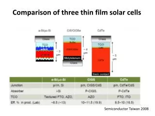
12 CIGS cells: a lower cost alternative (?) Sec. 7.6.1 Noufi, Rommel; Ken Zweibel. HIGH-EFFICIENCY CDTE AND CIGS THIN-FILM SOLAR CELLS: HIGHLIGHTS AND CHALLENGES. National Renewable Energy Laboratory.
13 Heterojunction advantages and problems E EC Wide bandgap window, but what happens at the interfaces? And why is CdS needed? EV x
A proposed band diagram www.tf.uni-kiel.de/...en/.../gerngross_reverey_paper_ws_08_1.pdf
Real heterostructures • What are the effects on the electrical properties of some previously unconsidered real surface effects? • surface reconstruction • dipole formation • interruption of the periodicity of the semiconductor • surface states