Download
1 / 57
580 likes | 607 Views
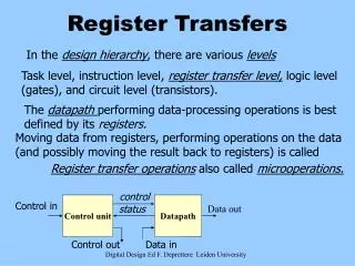
Register Transfers and Data Paths. Chapter 7 Mano&Kime. Datapaths and Operations. Digital systems are partitioned into two modules Data-path: perform data processing operations Control unit: determine the sequence of operations. Datapaths and Operations.

E N D
Register Transfers and Data Paths Chapter 7 Mano&Kime
Datapaths and Operations Digital systems are partitioned into two modules • Data-path: perform data processing operations • Control unit: determine the sequence of operations
Datapaths and Operations • Data paths are best defined by their registers and operations performed on data in the registers. • The movement of the data stored in the registers and the processing performed on the data are referred to as register transfer operations. The register transfer operations are specified by the following components. • The set of registers in the system • The operations performed on the data • The control that supervises the sequence of operations.
Datapaths and Operations • A register has the capability to perform one or more elementary operations such as • Load • Count • Add • Shift • The elementary operations performed on the data stored in the registers are called microoperations.
Register Transfer Operations • Register: a group of flip-flops, each of which is capable of storing one bit of information • RTL: The symbolic notation used to describe the micro-operation transfers among registers • Register representation: capital letters (sometimes followed by numerals)
register to register: R2 R1 • Memory to register: M[AR] DR (write) • DR M[AR] (read) Register Transfer Operations • Data Transfer: • Conditional Transfer (if-then): • If (K=1) then (R2 R1) • K1: R2 R1 • (K1 is any Boolean function that evaluates to 0 or 1)
Register Transfer Operations Any register transfer statement implies that circuit or hardware are available to perform the transfer. K1 is activated by the rising edge of a clock pulse at time t. At the next rising edge of the clock at time t+1, since load input K1 is active, R2’s data is loaded into R1 in parallel.
Microoperations Microoperations are classified as: • Transfer microoperations • Arithmetic microoperations • Logic microoperations • Shift microoperations
XK1:R1 R1 + R2 XK1:R1 R1 + R2 + 1 Arithmetic Microoperations • Consider the following statements: K1 activates an operation and X decides the operation type.
Logic Microoperations • Logic microoperations are useful for manipulating bits stored in registers. (K1 + K2): R1 R2 + R3, R4 R5R6
Logic Microoperations • AND operation is used to clear some of the bits in a register. 10101101 10101011 R1 (data) 00000000 11111111 R2 (mask) 00000000 10101011 R1 R1R2
Logic Microoperations • OR operation is used to set some of the bits in a register. 10101101 10101011 R1 (data) 11111111 00000000 R2 (mask) 11111111 10101011 R1 R1 R2
Logic Microoperations • XOR operation is used to complement some of the bits in a register. 10101101 10101011 R1 (data) 11111111 00000000 R2 (mask) 01010010 10101011 R1 R1 R2
Rn-1 Rn-2 R1 R0 Shift Microoperations • Logic shift-left/right: R0 shl/shr R0 - incoming bit is assumed to be “0” • Circular shift-left/right: R0 cil/cir R0 - rotate operation without any loss • Arithmetic shift-left/right: R0 ashl/ashr R0 - shift a signed binary number and leave the sign bit unchanged
Multiplexer Based Transfer • A register may receive data from two or more sources at different times. • Example If (K1 = 1) then ( R0 R1) else if (K2 = 1) then (R0 R2)
Bus-Based Transfer • A typical digital system has many registers. Paths must be provided to transfer data from one register to another. • The amount of logic and number of interconnections may be excessive if each register has its own dedicated set of multiplexers. • Bus: a set of common lines usually driven by selection logic to determine the path between source and destination - MUX-based bus and tri-state bus
Bus-Based Transfer 3n AND gates and n OR gates 4n gates in total 6n AND gates and 3n OR gates 9n gates in total
Three-State Bus • Three state bus construction has the potential for additional reduction in the number of gates, • It is especially effective in being bi-directional.
Three-State Bus There are only three data connections to to the set of register blocks for each bit of the bus. The multiplexer implemented bus has 6 connections for each bit to the set of register blocks.
Memory Number of bits in memory is referred as: K (kilo) - 210 M (mega) 220 G (giga) 230
Example 8388608 1048576 20 8 1024 10 4 4096 8388608 2097152 21 4 22 1 4194304 4194304 67108864 2097152 21 32 1048576 16384 14 64 8388608 23 8 67108864
Example 1024 X 16 memory 10 bits for addressing 16 bits for data
The steps for write are: Set the address lines Apply the data to the data input lines Activate the write input The steps for read are: Set the address lines Activate the read input Write and Read Operations
Memory Transfer Read: DR M[AR] Write: M[AR] DR Read: D1 M[A2] Write: M[A1] D2
Datapaths • Instead of having each register perform its microoperation ALU is shared. • The combination of a set of registers with a shared ALU and interconnecting paths is the datapath for the system.
Datapath • The control unit for the datapath directs the information flow through the buses, the ALU, the shifter and the registers by applying signals to the select inputs. Example for R1R2 + R3 the control signals needed are: A select (R2) B select (R3), MB select (0) G select for A+B MF select (0) MD select (0) Destination select (R1) Load enable
Datapath • The sets of values must be generated and must become available on the corresponding control lines early in the clock cycle. • The binary data from the two source registers must propagate through the multiplexers and the ALU and on into the inputs of the destination register, during the remainder of the same clock cycle. • Then when the next positive edge arrives , the binary data on bus D is loaded into the destination register.
The Arithmetic/Logic Unit • The ALU is a combinational circuit that performs a set of basic arithmetic and logic microoperations.
Logic Circuit • The logic operations are bitwise operations: • - Implemented by AND, OR, XOR and NOT gates • with a 4 to 1 MUX, bit by bit. • - Logic simplification reduces the gate count
The Shifter S=00 no shift S=01 shift right S=10 shift left