Download
1 / 12
170 likes | 558 Views
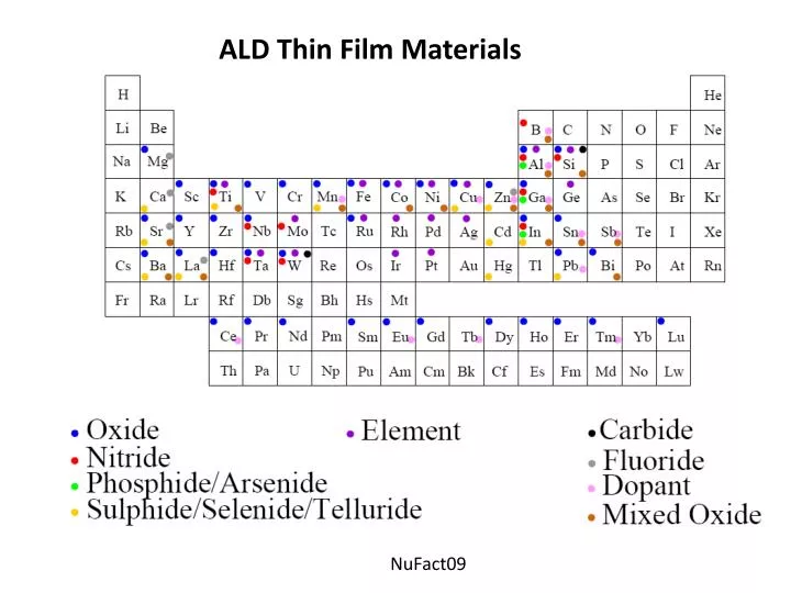
ALD Thin Film Materials. LDRD review 2009. NuFact09. ALD of III-V semiconductors and other structure/materials. What have been done: - GaN - AlN - AlGaN - InN Not too hard for InGaN -TiO 2 - ZnO Other: Pt nanoparticles Ag nanoparticles. Cutoff at 380 nm, up to 50% QE at 310 nm.

E N D
ALD Thin Film Materials LDRD review 2009 NuFact09
ALD of III-V semiconductorsand other structure/materials What have been done: -GaN -AlN -AlGaN -InN Not too hard for InGaN -TiO2 -ZnO Other: Pt nanoparticles Ag nanoparticles Cutoff at 380 nm, up to 50% QE at 310 nm BiAlkali’soverlayer for e- emission Absorb at 380nm but surface defect -> re-emits at ~ 540 nm + broad Fill defect on oxide : very high absorption at 380 nm very high absorption above 1000 nm
Home made: -Transfer: Open in air -> issue -No vacuum inside the ALD chamber -Only Thermal ALD Atomic Layer deposition Commercial: -Load lock + glove bag: Inert gas (N2, Ar…) for sample transfer -In-situ characterization: Ellipsometry Mass spec QCM and maybe IR spec -In-situ vacuum post annealing -ALD + Plasma ALD
Mixed Layer Growth • Layer by Layer • note “steps” • atomic layer sequence “digitally” controlled ZnO [(CH3CH2)2Zn // H2O] [(CH3)3Al // H2O] Al2O3 ZnO Al2O3 • Mixed Layers w/ atomic precision • Low Temperature Growth • Transparent • Uniform • Even particles in pores can be coated. 100 nm • Films Have Tunable Resistivity, Refractive Index, Surface Roughness, etc. Mixed Oxide Deposition: Layer by Layer LDRD review 2009 NuFact09
ZnO Si 200 nm 1 μm ZnO in Silicon High Aspect Ratio Trench • ALD is very good at coating non-planar surfaces
Argonne ALD facilities: Plasma ALD (PEALD) Elemental Metals: Al, Cu, W, Mo… & alloys: NbN, TiN, Pt/Ir etc… Purer materials-> bulk properties • -Bi Alkalies: • CsI3 (g) + H2 (plasma) = CsI + 2HI (g) • GeCl4 (g) + 2H2(plasma) = Ge + 4HCl (g). • 2SnCl5 (g) + 10H2 (plasma) = 2Sn + 10 HCl (g).
Work for both Plasma and regular ALD. Light, λ≤400 nm ITO, conducting-transparent oxides, or Pt, W, Cu, Mo etc.. With plasma ALD Mean free path e-hole l < d d Light absorption layer Need Cs layers for QE~50 to 70% e- MCP
Light, λ≤400 nm ITO for bias ~ few Volts d~50nm, e- d’< l d’~ 10 nm Metallic wires -> field enhancements: Nanotubes… Thermal Noise ? Al2O3 Diamond? MCP Metallic layer -Nanotubes + free space filled with TiO2 - “AAO” type membrane made out of TiO2 + ALD filled with metals - AAO membrane filled with both: light absorber and metal
45 nm Ag nano-particles AAO e- e- λ e- e- MCP Al nano-films
absorption Metallic electrode e- MCP -Cannot use ALD -> coat inside the tube too -Plasma ALD -> lower aspect ratios, controlled by plasma exposure time
Light, λ≤400 nm Surface plasmon: Gold nanoparticules Light, λ~600 nm e- MCP