Download
1 / 24
240 likes | 250 Views
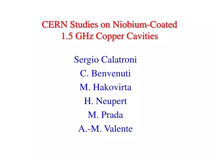
CERN Studies on Niobium-Coated 1.5 GHz Copper Cavities. Sergio Calatroni C. Benvenuti M. Hakovirta H. Neupert M. Prada A.-M. Valente. Outline of the talk. Motivation for the study: the high-field residual resistance Thermal effects Surface defects and roughness

E N D
CERN Studies on Niobium-Coated1.5 GHz Copper Cavities Sergio Calatroni C. Benvenuti M. Hakovirta H. Neupert M. Prada A.-M. Valente
Outline of the talk • Motivation for the study: the high-field residual resistance • Thermal effects • Surface defects and roughness • Role of the grain size and purity • Hydrogen studies: • RF measurement • Thermodynamics • Conclusions
Motivation: the high-field residual resistance Coatings performed using krypton on electropolished spun copper cavities (Santa Fe 1999) Limited by RF power
Testing: higher field operation The performance can be extended straightforwardly at higher fields Limited by RF power (250 W) (Thermal instability of the standard small cryostat is not a limiting issue)
Testing: thermal effects In Nb/Cu cavities we must cope with several thermal impedances: Cu/He (~6000 W/m2K), across Cu (negligible), Nb/Cu interface (?), across Nb film (negligible) If the Rs increase would only be due to some heating of the film -> RBCS It is then possible to estimate the temperature increase that corresponds to the measured Rs increase. The dissipated power is also easily calculated A Kapitza-like mechanism would give a straight line in the plot
Surface defects & roughness 2.0 µm 2.0 µm Chemically polished copper • average roughness: 0.2 mm • pinholes of 0.3 mm Electropolished copper • average roughness: 0.02 mm • nearly no defects
Irregularities on the substrate surfaceshadowing effect film inhomogeneities He leak rate experiment ‹inc› fraction of leakyfilm surface - equator 9° 4.4 ppm - (~iris 50° 25 ppm) - equator 9° 0.1 ppm CP EP Surface defects: measurement of pinholes Substrate disk Machining and cleaning Film deposition Substrate removal p1 p2 film
Copper roughness I: electropolishing The window of optimum polishing parameters is rather narrow. Reproducing these parameters over the entire surface of the cavity cell needs further R&D Production of O2 bubbles! Production of Cu(OH)2 on the surface!
Copper roughness II: electropolishing • Electropolishing parameters: • 55% vol. H3PO4 • 45% vol. butanol • Current density: 200A/m2 • HP water rinsing Electropolishing with a quasi-homotetic cathode has replaced chemical polishing (LEP standard) for surface preparation.
Copper roughness III: electropolishing current density is 5 times larger at iris current density is identical The electropolishing cathode is being optimised by means of a sophisticated computer simulation code. The current density can be made uniform
80 70 degrees 60 50 40 30 20 10 0 10 20 30 40 50 Intrinsic film roughness & incidence angle of the niobium atoms mm 50 mm 0 mm
Intrinsic film roughness: incidence angle and residual resistance An issue which is of great interest also for low-ß cavities, is the correlation between the incidence angle of the film and the residual resistance
Digression: new ideas for low-beta cavities coating Nb ring Cu half-cell Problem: coating incidence angle in low-beta cavities Solution: coat at favourable angle before welding
Properties of the coatings I : grain size with FIB micrographs Standard films Oxide-free films 0.5 µm 0.5 µm Courtesy: P. Jacob - EMPA
Properties of the coatings II: purity, Hc1, texture, etc... StandardOxide-free RRR 11.5 ± 0.1 28.9 ± 0.9 TC9.51 ± 0.01 K 9.36 ± 0.04 K Ar cont. 435 ±70 ppm286 ± 43 ppm Texture (110) (110), (211), (200) Hc185 ± 3 mT31 ± 5 mT Hc21.150 ± 0.1 T0.73 ± 0.05 T a03.3240(10)Å 3.3184(6) Å Da/a0.636 ± 0.096 % 0.466 ± 0.093 % Stress -706 ± 56 MPa-565 ± 78 MPa Grain size110 ± 20 nm> 1 µm
Properties of the coatings III: effect on residual resistance OX: oxidised copper substrate OF: oxide-free copper substrate CP: chemical polishing EP: electropolishing • Oxide-free films (larger grains, better purity, less stress, etc...) have on average a larger residual resistance (measured at low field) • In contrast with models linking the residual resistance with Josephson dissipation at grain boundaries
Hydrogen studies I: film loading • Spun cavities coated using argon as sputter gas loaded with 1.4 at.% of hydrogen Hydrogen loading induces a much larger degradation for oxide-free films
Hydrogen studies II: outgassings Question: why were coatings on oxide-free hydroformed cavities consistently worse than for spun cavities? (Legnaro 1997) Possible answer: a larger quantity of hydrogen was migrating into the film from the hydroformed cavity
Hydrogen studies III: outgassings Bare Cu The hydrogen content and has been measured also by thermal outgassing to 350 ºC, for passivated and non-passivated Nb films (i.e. NbxOy at the surface) Oxidised copper:2200±200 ppm 800±200 ppm Oxide free: 2000±200 ppm 980±200 ppm
Hydrogen studies IV: isosteres Oxidised copper pH2(cH)2exp(-EH/kT) The hydrogen content and its binding energy with the lattice can be measured with isosteric cycles and successive injections of known quantities of hydrogen. Oxidised copper: 400±200 ppm340±10 meV/at Oxide free: 1000±200 ppm320±10 meV/at
Digression: HPWR I Nb/Cu film on CP copper HPWR effectively reduces Rres0 (1999 result)
Digression: HPWR II 10 µm 10 µm Before HPWR After HPWR Bulk Nb - EP with KEK bath HPWR smoothens the grain boundaries (2001 results)
Conclusions • The maximum field of Nb/Cu cavities is not limited by any intrinsic phenomena. • However, the residual resistance suffers from a steep increase at high field (threshold ~15 MV/m). • Several possible causes have been investigated. The most probable sources are: surface defects, hydrogen content. • Possible cures are: better electropolishing (under way), reducing hydrogen content (difficult). • Coating for low-beta cavities are being addressed with a suitable modification of the sputtering technique.