Download
1 / 22
250 likes | 553 Views
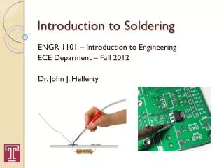
EMS1EP Lecture 3 Intro to Soldering. Dr. Robert Ross. Overview (what you should learn today). What are Printed Circuit Board (PCB’s) How PCB are made Different types of PCBs What is soldering How to solder. What are Printed Circuit Boards.

E N D
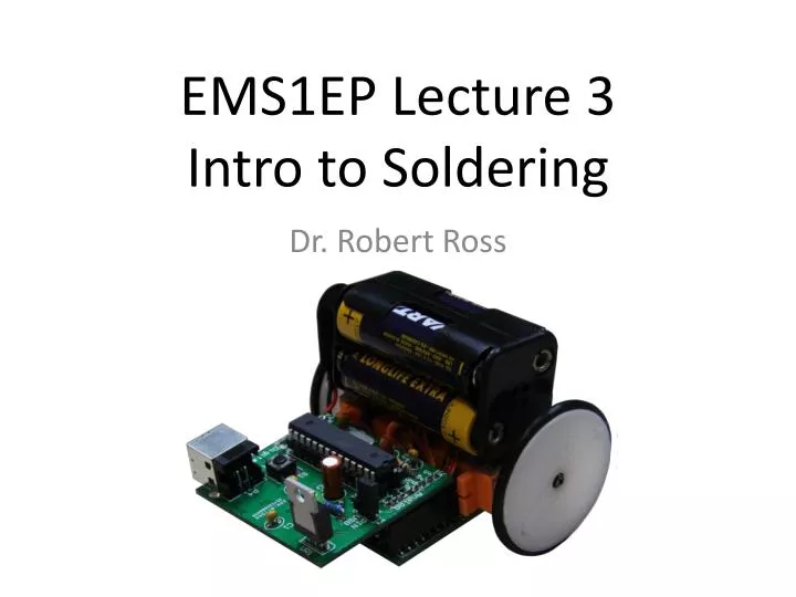
EMS1EP Lecture 3Intro to Soldering Dr. Robert Ross
Overview (what you should learn today) • What are Printed Circuit Board (PCB’s) • How PCB are made • Different types of PCBs • What is soldering • How to solder
What are Printed Circuit Boards • PCBs consist of a surface which is plated with a conductive material (like copper) • Components can be soldered directly onto the conductive material • This supports components and connects them to each other to form a circuit
Some PCB terms • Track: the copper traces between pads • Pad: what components are soldered to • Via: an electrical connections between different layers of the board • Footprint: the mechanical relationship between the pads for a specific component • Plane: not just traces but whole regions which connect pads together
How PCBs are made Several different techniques, most common are: • Silk screen • Photo engraving • PCB milling As part of the process a drill is then used to create all the holes to put components and screws through
Silk Screen PCB • Board (typically fiberglass FR4) is covered with a thin layer of copper foil • Any tracks and pads (copper we want to keep) is covered in etch-resistant ink • The remaining copper is then chemically etched away
Photoengraving • Copper layer on board is covered with a light-sensitive ink • A photomask is placed onto the board and the board is exposed to UV light • The remaining copper is then chemically etched away • Finer resolution compared to silk screening process
PCB Milling • A 3-axis mechanical milling machine is used to cut away unwanted copper • High speed motor drives a cutting bit which cuts away the copper • Not as accurate and trickier for multi-layer PCBs • Automates hole drilling
Solder Mask • Any part of the exposed copper can be soldered • Generally we only want to solder where we attach components • A solder mask (non-conductive layer) is added to the board leaving the solder pads exposed • Prevents oxidation and solder bridges between close tracks
Overlay • An overlay can be applied over the solder mask • This is the writing which is useful for humans to read for assembly and maintenance • Generally using a silkscreen (white is the most common overlay colour)
Multilayer PCBs • A single piece of fibreglass can be coated on the front and back with copper – this is a 2-layer PCB • For more layers boards can be made separately and laminated together • This gives more layers that tracks can be mounted on • Often whole layers are selected as ground layers which improves noise performance • Vias connect between the different layers • 4 and 6 layer boards are common, can go up to around 38 layers
How PCBs are designed • Design schematic in CAD software (we use Altium) • Layout and route board in CAD software (Altium) • Many different routing possibilities • Auto routing • Guidelines: • Ground plane (avoid large loops) • Wider tracks for power • Avoid right angles
What is soldering • Soldering is a way of making electrical connections • It involves melting solder (an alloy of tin and lead) to form a bond between the conductors on different components
Soldering Precautions • Never touch the hot end of the soldering iron (~370oC) • If you do get burnt run your finger under cold water for 5 minutes • Don’t burn the table, the power leads, keyboards, your classmates • Don’t melt anything except solder • When not in use put the soldering iron back on the stand (not on the table)
Soldering Precautions • Wear safety glasses, solder can flick into your eye • Wash your hands well after soldering (solder is 40% lead) • Use the fume extractors and don’t breath in the solder fumes
How to solder • Hold the soldering iron like a pencil • Clean the soldering iron (wet sponge or brass strands) before you use it (if it hasn’t be used for more than 60 seconds) – it should look shiny
How to solder • Hold the tip on the component lead and pad • Add solder and let it flow into the joint • Remove the solder • Remove the soldering iron and allow joint to cool (5 sec) before moving anything
Soldering Video Demo • http://www.youtube.com/watch?v=euw9tkxBgus
Through-hole/Surface Mount • 2 types of components: • Through hole: have leads which pass through holes on the PCB and are soldered on other side • Surface Mount (SMT) soldered onto the same side of the PCB that the component is on • SMT tends to be much smaller allowing greater miniaturisation of electronics
Desoldering • If something goes wrong – don’t worry solder will remelt • Techniques to removing components: • Reheat and pull component out • Desoldering braid (braid draws solder away from joint) • Desoldering gun (sucks hot solder from joint) • Hot air (heats all the pads using hot air)
Summary(What you learnt in this session) • Printed Circuit Boards (PCBs) are the most common method used to implement electronic circuits • Soldering is how we make the electrical connections between components and the PCB