Download

1 / 24
270 likes | 326 Views
Shift Register. Shift Register. Objectives Upon completion of this chapter, you will be able to : Explain the different classifications of registers : Parallel In / Parallel Out Serial In / Serial Out Parallel In / Serial Out Serial In / Parallel Out Construct register using RS flip-flop

E N D
Shift Register Shift Register
Objectives Upon completion of this chapter, you will be able to : • Explain the different classifications of registers : • Parallel In / Parallel Out • Serial In / Serial Out • Parallel In / Serial Out • Serial In / Parallel Out • Construct register using • RS flip-flop • D flip-flop • Determine the number of flip-flops required for an N-bit shift register
Introduction Shift Register is a Digital circuit that accepts binary data from some input source and then shifts these data through a chain of flip-flops one bit at a time.
The various types of registers can be classified according to the manner in which data can be entered into the register for storage and the manner in which data are outputted from the register. The various classifications are listed below • Parallel In / Parallel Out ( 74174, 74LS174 ) • Serial In / Serial Out ( 7431B ) • Parallel In / Serial Out ( 74165, 74LS165 ) • Serial In / Parallel Out ( 74164, 74LS164 ) Each of these types is available in IC form so that a logic designer can usually find exactly what is required for a given application.
Parallel In/ Parallel Out Serial In/ Serial Out Parallel In/ Serial Out Serial In/ Parallel Out Shift Register Tutorial
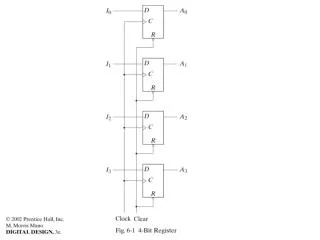
It is a 6-bit register that has parallel inputs D0 through D5 and parallel outputs Q0 through Q5. Parallel data are loaded into the register on the PGT of the clock input CP. A master reset input MR can be used to asynchronously reset all the register FFs to 0. 1 Parallel In / Parallel Out (74174, 74LS174 )
D5 D4 D3 D2 D1 D0 CP MR 74174 /LS174 / HC174 Q5 Q4 Q3 Q2 Q1 Q0 CP MR D5 D4 D3 D2 D1 D0 D D D D D D Q Q Q Q Q Q CP CP CP CP CP CP CLR CLR CLR CLR CLR CLR Q5 Q4 Q3 Q2 Q1 Q0
Parallel In / Parallel Out (74174, 74LS174 ) The data at the input will be shifted to the outputonly when the register gets the clock pulse, PGT. MR CP D5 D4 D3 D2 D1 D0 D5=1 D4=1 D3=1 D2=0 D1=0 D0=0 D D D D D D Q Q Q Q Q Q CP CP CP CP CP CP CLR CLR CLR CLR CLR CLR Q5 =1 Q4=1 Q3=1 Q2=0 Q1=0 Q0=0 Q5 Q4 Q3 Q2 Q1 Q0
A master reset MR can be used to reset all the register Parallel In / Parallel Out (74174, 74LS174 ) MR CP D5 D4 D3 D2 D1 D0 D5=1 D4=1 D3=1 D2=0 D1=0 D0=0 D D D D D D Q Q Q Q Q Q CP CP CP CP CP CP CLR CLR CLR CLR CLR CLR Q5 Q4 Q3 Q2 Q1 Q0 Q5 Q4 Q3 Q2 Q1 Q0 Q5 =1 Q4=1 Q3=1 Q2=0 Q1=0 Q0=0 Main Menu
The End MAIN MENU
2 Serial In / Serial Out (7431B) It is a CMOS quad 64-bit shift register. It contains four identical 64-bit shift registers on one chip. It has a serial input, DS, a clock input CP that responds to NGTs, and a serial output from the last FF, Q63 . Q63 is the only output that is externally accessible. This output goes through a buffer circuit ( triangle symbol with no inversion bubble). A buffer does not change the signal’s logic level; it is used to provide a greater output-current capability than normal.
Q Q Q Q D D D D Ds FF0 FF1 FF2 FF3 CP CP CP CP CP Q Q Q Q D D D D FF60 FF61 FF62 FF63 CP CP CP CP Q63 Logic diagram for one of four 64-bit shift registers on a 4731B
0 1 1 0 1 1 1110001110 11100011100 1110001110001 111000111000 11100011100011 111000111000111 Q Q Q Q D D D D Ds FF0 FF1 FF2 FF3 CP CP CP CP CP Q Q Q Q D D D D FF60 FF61 FF62 FF63 CP CP CP CP Q63 The data at the input will only be shifted into the register when there is a clock signal.
The End MAIN MENU
It is an 8-bit shift register. It has both serial data entry via DS, and parallel data entry via P0 through P7. The only accessible FF outputs are Q7 and Q7 . The FFs are clocked SR type that respond to NGTs at their clock inputs. Each FF has asynchronous inputs, PRESET and CL, that are used for parallel data entry. There are two clock inputs, CP1 and CP2, either of which can be used to produce the shift operation on PGTs. 3 Parallel In / Serial Out (74165, 74LS165)
P0 P1 P2 P3 P4 P5 P6 P7 DS CP1 CP2 PL Q7 Q7 74165 P0 P1 P2 P3 P4 P5 P6 P7 DS CP1 CP2 PL PRESET S Q0 CP R Q0 CL PRESET S Q1 CP R Q1 CL PRESET S Q2 CP R Q2 CL PRESET S Q3 CP R Q3 CL PRESET S Q4 CP R Q4 CL PRESET S Q5 CP R Q5 CL PRESET S Q6 CP R Q6 CL PRESET S Q7 CP R Q7 CL
The End MAIN MENU
It is an 8-bit shift register. Each Flip-Flop output externally accessible. An AND gate combines inputs A and B to produce the serial input to flip-flop Q0 . The shift operation occurs on the PGTs of the clock input CP. The MR input provides asynchronous resetting of all FFs on a LOW level. 4 Serial In / Parallel Out ( 74164, 74LS164 )
A B CP MR D Q CP CD D Q CP CD D Q CP CD D Q CP CD D Q CP CD D Q CP CD D Q CP CD D Q CP CD A B CP 74164 / 74LS164 Q0 Q1 Q2 Q3 Q4 Q5 Q6 Q7 MR
The End MAIN MENU
18 24 30 28 27 26 25 23 10 22 29 20 19 17 16 15 14 13 12 11 21 9 1 0 8 2 5 4 6 7 3 Q 1 What kind of register can have a complete binary number loaded into it in one operation, and then have it shifted out one bit at a time? A) Parallel In / Parallel Out B) Serial In / Serial Out C) Parallel In / Serial Out D) Serial In / Parallel Out
18 24 30 28 27 26 25 23 10 22 29 20 19 17 16 15 14 13 12 11 21 9 1 0 8 2 5 4 6 7 3 Q 2 What type of register can have data entered into it only one bit at a time, but has all data bits available as outputs? A) Parallel In / Parallel Out B) Serial In / Serial Out C) Parallel In / Serial Out D) Serial In / Parallel Out
18 24 30 28 27 26 25 23 10 22 29 20 19 17 16 15 14 13 12 11 21 9 1 0 8 2 5 4 6 7 3 Q 3 In what type of register do we have access only to the leftmost and rightmost FFs? A) Parallel In / Parallel Out B) Serial In / Serial Out C) Parallel In / Serial Out D) Serial In / Parallel Out
The End MAIN MENU