Download
1 / 4
210 likes | 805 Views
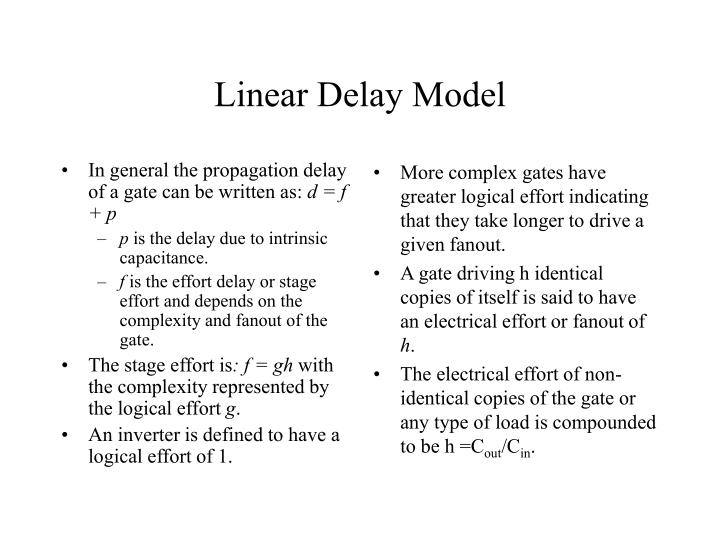
In general the propagation delay of a gate can be written as: d = f + p p is the delay due to intrinsic capacitance. f is the effort delay or stage effort and depends on the complexity and fanout of the gate.

E N D
In general the propagation delay of a gate can be written as: d = f + p p is the delay due to intrinsic capacitance. f is the effort delay or stage effort and depends on the complexity and fanout of the gate. The stage effort is: f = gh with the complexity represented by the logical effort g. An inverter is defined to have a logical effort of 1. More complex gates have greater logical effort indicating that they take longer to drive a given fanout. A gate driving h identical copies of itself is said to have an electrical effort or fanout of h. The electrical effort of non-identical copies of the gate or any type of load is compounded to be h =Cout/Cin. Linear Delay Model
Logical effort of a gate is defined as the ratio of the input capacitance of the gate to the input capacitance of an inverter that can deliver the same output current. Assuming that the pMOS has twice the resistance of an nMOS we have Cin(inv) = 3 for inverter that achieves symmetric switching. The logical effort of an inverter is: g =3/3 =1. How well can we design a NAND or NOR gate to give the output current equal to that of a unit inverter? NAND: Cin for unit inverter is 3 units while that of the NAND is 4 units for each input. Logical effort for NAND is 4/3. The NOR gate has Cin of 5 units and thus has a logical effort of 5/3. Determine the logical effort of a 3-input NAND Logical Effort
The parasitic delay of a gate is the delay of a gate when it drives zero load. A quick estimation of parasitic delay computations only accounts for the diffusion capacitance of the output node. The inverter has 3 units of diffusion capacitance on the output with each transistor having resistance R. Its parasitic delay becomes 3RC The normalized parasitic delay of an inverter is 1 and will be referenced as pinv. pinv is the ratio of the output capacitance to the input capacitance. The parasitic delays of the NAND and NOR gates is twice that of the inverter (2pinv), because they each have 6 units of diffusion capacitance. Note that internal node capacitances have been ignored. Parasitic Delay
Parasitic delay grows more than linearly with an increase in the number of inputs in a real NAND or NOR circuit. tpd =R(3nC)+Sumn-1i=1(iR/n)(nC)=(n2/2+5n/2)RC In practice it is advisable to keep n=4 as seen that tpd grows quadratically with n. Series n-type devices are better than series p-type devices. Why? The linear model does not account for the slopes of the input and output signals (assumes zero rise and fall times). The input arrival times is not accounted for. The inputs do not simultaneously switch ON and OFF. The Elmore Model