Download
1 / 15
150 likes | 281 Views
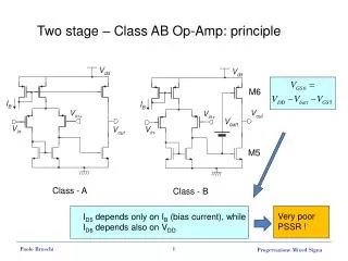
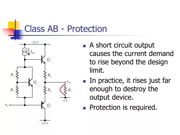
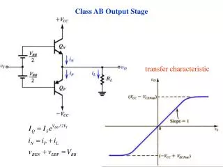
Class AB - Protection. A short circuit output causes the current demand to rise beyond the design limit. In practice, it rises just far enough to destroy the output device. Protection is required. Short Circuit Protection.

E N D
Class AB - Protection • A short circuit output causes the current demand to rise beyond the design limit. • In practice, it rises just far enough to destroy the output device. • Protection is required.
Short Circuit Protection • Normally, VRE» .05 V (<< 0.5V) so Q4 stays off and does not interfere. • If IC1 rises above the normal maximum, however, VRE rises and Q4 turns on, diverting Ibias and, therefore, switching off Q1.
Class C Operation Iout Time One device conducts for a small portion of the a.c. cycle. Conduction angle << 180 °.
A Class C Output Stage • Class C power amplifier relies on a narrow band tuned load. • Transistor only conducts when vin > VBIAS + VBE. • For the remainder of the a.c. cycle, current circulates around the tuned load.
Class C Output Waveforms Input Output
Transistor Dissipation Three operating regions:
Class C Efficiency • For most of the a.c. cycle, the transistor is off – i.e. zero power dissipation. • When it is on, it is close to saturation – i.e. VCE is low implying low power dissipation. • Average power dissipation is much lower than output power so efficiency can be > 99 %.
Class D Operation • A Class D amplifier varies its output voltage using pulse width modulation. • The mark-space ratio of a high frequency square wave is set to be proportional to the required output. • The average output voltage can be recovered by a low pass filter.
A Class D Output Stage P.W.M. L.P.F RL
Class D Efficiency • Each of the two transistors in a class D output stage is always either fully on (saturated) or fully off. • When on, VCE is close to zero so power dissipation is approximately zero. • When off, IC is zero so power dissipation is zero again. • In theory, efficiency ≈ 100 %.
PD t Class D Inefficiency Most power dissipation will be during the transitions between states. IC t VCE t
Minimising Class D Inefficiency • Fast switching is essential for low power dissipation. • Low PWM frequency implies fewer transitions and lower power dissipation… • …but PWM frequency shouldn’t be so low that the output is distorted.
Output Stage Selection • Class A – low complexity, good linearity but poor efficiency. Usually suitable for low power only. • Class B – High efficiency, suitable for switching applications. • Class AB – High efficiency and linearity. Good general purpose power amp. • Class C – Very efficient for high-Q loads. • Class D – Very efficient but complex.
Power Amplifiers – Key Issues • Output Stage Selection. • Linearity / Distortion • Efficiency • Power Dissipation. • Heatsink Requirements. • Thermal resistance • Junction temperature • Biasing / Thermal Runaway. • Class AB design of Vbias • Protection.

![Class 3 Ab + L AbL Review d/ dt [ AbL ] = k on [ Ab ][L] – k off [ AbL ]](https://cdn1.slideserve.com/3152792/slide1-dt.jpg)