Download
1 / 10
100 likes | 179 Views
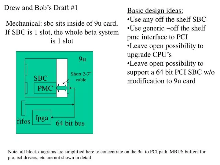
Drew and Bob’s Draft #1. Basic design ideas: Use any off the shelf SBC Use generic ~off the shelf pmc interface to PCI Leave open possibility to upgrade CPU’s Leave open possibility to support a 64 bit PCI SBC w/o modification to 9u card. Mechanical: sbc sits inside of 9u card,

E N D
Drew and Bob’s Draft #1 • Basic design ideas: • Use any off the shelf SBC • Use generic ~off the shelf pmc interface to PCI • Leave open possibility to upgrade CPU’s • Leave open possibility to support a 64 bit PCI SBC w/o modification to 9u card Mechanical: sbc sits inside of 9u card, If SBC is 1 slot, the whole beta system is 1 slot 9u SBC Short 2-3” cable PMC fpga fifos 64 bit bus Note: all block diagrams are simplified here to concentrate on the 9u to PCI path, MBUS buffers for pio, ecl drivers, etc are not shown in detail
WCK WCK RCK RCK FIFO FIFO WEN WEN REN REN Drew and Bob’s Draft #1 Block Diagram PMC Drivers Bidirectional 64 bit bus for PIO, etc One direction for DMA 64 9u card 13 Control/Arb 64 64 128 Altera 10K100 MBDA MBAD 32 12 To Hlink? MBARB 32 Drivers 12 To Hlink? P2 Lines 16 33 To ECL
Drew and Bob’s Draft #1 Comments: We included new drivers on the PMC and drivers on the 9u card because we expected that the TTL from the fifo’s, FPGA, and PMC might not be able drive the cable. I’m not sure this is a problem after giving it more thought… (more later) The FPGA model here is that the PMC card’s FPGA serves as a bridge between the local bus of the PCI interface and the private bus used to connect the PMC w/ the FPGA on the 9u card. The 9u FPGA replaces the PIO/DMA/ and TSI devices and maybe also provides a new hotlink output. It also supports a custom interface to the PMC card.
Orsay Draft • Basic design ideas: • A single fpga can do the job instead of programming two of them • do away / PMC + cable • do away w/ drivers by keeping signal paths short in this design • Choose one off the shelf and • 9u card layout is done to mate w/ this board Mechanical: SBC sits under the 9u card. Its PMC connector plugs into the bottom of the 9u board, the is no PMC card – this eats two slots minimum. 9u SBC Pci controller on 9u card No cable – hard, fixed connector to SBC pmc conn 32 bit bus localbus fpga fifos “piggyback” of SBC onto 9u card
WCK WCK WCK WCK RCK RCK RCK RCK FIFO FIFO FIFO FIFO WEN WEN WEN WEN REN REN REN REN Orsay Draft Block Diagram AMCC PCI Interface 9u card 32 A/D + Control/Arb PCI interface local bus 32 128 Altera 20K200 Local bus module MBDA MBAD 32 MBARB 32 Drivers P2 Lines 16 33 To ECL
Orsay Draft Comments: One card to build, all function is on 9u card. Only one local/private bus to control. No differential drivers used – FIFO output is buffered through FPGA, and bus lengths are kept short <~ 20 cm, so TTL can drive w/ no problems at 33MHz (local bus speed = PCI bus speed) The 9u FPGA replaces the PIO/DMA/ and TSI devices. It now serves as the local bus interface.
Bob/Drew + use ~any SBC at any time + 64-bit connection from 9u card allows added upgrade path for SBCs + mechanicals similar to standard VME extender board -two FPGA’s to program -two bus protocals -two boards to build (IF the cern card needs new drivers added…) Orsay + one card to build +1 fpga to program +1 local bus protocal +all TTL interface to SBC (no differential drivers) -fixed choice of SBC -essentially no upgrade path w/o major redesign -personal opinion odd mechanicals
A Combination of both drafts Block Diagram • I think the strengths of both designs can be combined as follows: • Route the output of the FIFO’s through the FPGA for some added buffering instead of asking them to drive the bus on the 9u card and the cable - this should keep max distances to <~ 20cm for any TTL output • Now we could actually use the CERN card w/ no modification at all. There are two ways to implement this • Put a mindless program in the PMC fpga to pass the PCI controller’s local bus straight out of the card. Then the 9u fpga will include a module to drive the local bus (33MHz w/ a 32 bit data width) ala ORSAY’s idea. • Go w/ a 64 bit private bus as planned and to some work in the PMC FPGA as we initially proposed (this could be done much later, as a upgrade project, if we don’t want to do it initially!) and build a higher bandwidth private bus
WCK WCK RCK RCK FIFO FIFO WEN WEN REN REN A Combination of both drafts Block Diagram PMC 64 9u card 77 Control/Arb + 64 bits data 64 64 128 Altera 10K100 MBDA MBAD 32 12 To Hlink? MBARB 32 Drivers 12 To Hlink? P2 Lines 16 33 To ECL
Combined Design + still only have to design one card (PMC and SBC are truly off the shelf) + trivial option for PMC FPGA coding (just pass local bus) + all future upgrade advantages are still available i.e. maximum future flexibility w/o a significantly larger design/firmware effort + Firmware upgrades on 9U card can support HARDWARE upgrades on PMC/SBC cards