Download
1 / 1
30 likes | 235 Views
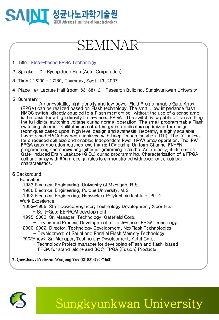
SEMINAR. 1 . T itle : Flash-based FPGA Technology 2. S peaker : D r. Kyung Joon Han (Actel Corporation) 3. T ime : 1 6 :00 – 17:30, Thursday, Sept. 13, 2007 4. P lace : e+ Lecture Hall (room 83188), 2 nd Research Building, Sungkyunkwan University 5. Summary :

E N D
SEMINAR 1. Title : Flash-based FPGA Technology 2. Speaker : Dr. Kyung Joon Han (Actel Corporation) 3. Time : 16:00 – 17:30, Thursday, Sept. 13, 2007 4. Place : e+ Lecture Hall (room 83188), 2nd Research Building, Sungkyunkwan University 5. Summary : A non-volatile, high density and low power Field Programmable Gate Array (FPGA) can be realized based on Flash technology. The small, low impedance flash NMOS switch, directly coupled to a Flash memory cell without the use of a sense amp, is the basis for a high density flash-based FPGA. The switch is capable of transmitting the full digital switching voltage during normal operation. The small programmable Flash switching element facilitates use of a fine grain architecture optimized for design techniques based upon high level design and synthesis. Recently, a highly scalable flash-based FPGA has been achieved with Deep Trench Isolation (DTI). The DTI allows for a reduced cell size and enables Independent Pwell (IPW) array operation. The IPW FPGA array operation requires less than 10V during Uniform Channel FN-FN programming and shows negligible programming disturbs. Additionally, it eliminates Gate-Induced Drain Leakage (GIDL) during programming. Characterization of a FPGA cell and array with 90nm design rules is demonstrated with excellent electrical characteristics. 6 Background : Education 1983 Electrical Engineering, University of Michigan, B.S 1986 Electrical Engineering, Purdue University, M.S 1992 Electrical Engineering, Rensselaer Polytechnic Institute, Ph.D Work Experience 1993-1995: Staff Device Engineer, Technology Development, Xicor Inc. - Split-Gate EEPROM development 1995-2000: Sr. Manager, Technology, Gatefield Corp. - Device and Process Development of flash-based FPGA technology. 2000-2002: Director, Technology Development, NexFlash Technologies - Development of Serial and Parallel Flash Memory Technology 2002-now: Sr. Manager, Technology Development, Actel Corp. - Technology Project manager for developing eFlash and flash-based FPGA for stand-alone and SOC-FPGA (Fusion) Products 7. Questions : Professor Wonjong Yoo (☏ 031-290-7468) Sungkyunkwan University