Download
1 / 43
430 likes | 556 Views
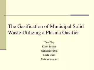
Plasma Television Service Seminar Circuit Explanation for PX60/PX600. 2006 PDP Line-up. 2006. 2005. TH-58PX600. HD Step Up Model. TH-50PX600. TH-50PX500. TH-42PX600. TH-42PX500. TH-58PX60. TH-50PX50. TH-50PX60. HD Leader Model. TH-42PX50. TH-42PX60. TH-37PX50. TH-37PX60.

E N D
Plasma Television Service Seminar Circuit Explanation for PX60/PX600
2006 PDP Line-up 2006 2005 TH-58PX600 HD Step Up Model TH-50PX600 TH-50PX500 TH-42PX600 TH-42PX500 TH-58PX60 TH-50PX50 TH-50PX60 HD Leader Model TH-42PX50 TH-42PX60 TH-37PX50 TH-37PX60 SD Leader Model TH-42PD60 TH-42PD50
Summary of PD60, PX60, PX600 58” 50” 50” 42” 42” Advanced Smart Sound New O ----- ----- SOUND Hi-end Leader PX600 PD60 PX60 50/58” 42” 42” 37” New Panel SD HD HD GP9DE Digital Tuner O O O DT O ----- ----- Cable Card / TV guide O ----- O JPEG Photo Viewer SD Card ----- ----- ----- JPEG Photo Viewer PC Card New 1 2 2 HDMI w/HDAVI Control(*) ----- ----- O PC Input O ----- ----- Multi Window
Current 50PX500/PX50 New 50PX600/PX60 C1 C2 C3 C1 C2 C3 SS2 SS2 PB P P PA Fan Control SU SU Power Power D Audio Power DC - DC - Supply Supply Different Points form 2005 models (50”) Format Converter Converter SS Plasma AI Processor SS SC SC Sustain Sustain DG DT DG Drive Drive Scan Drive Scan Drive PA DT Digital Z D-TV Interface Signal DC - DC - D-TV Interface Audio Processor Converter DV Amp SD SD H HDMI D SS3 SS3 H AV Terminal HC AV Terminal C6 C5 C4 C6 C5 C4 G GK GS GS G GK K S K S Front Terminal Front Terminal PC Card SD Card SD Card Key SW Key SW REMOTE, LED POWER SW REMOTE, LED POWER SW PX500only Different points from current design 1. Eliminated PB and Z board 2. Changed PA and D board position 3. HDMI terminals on DG board 4. Added HC board(factory use)
Current 42/37/PX500/PX50/PD50 New 42/37/PX600/PX60/PD60 C1 C2 SS2 PB P P PA Fan Control SU SU Power Power D Audio Power DC - DC - Supply Supply Converter Different Points form 2005 models (37”/42”) Format Converter SS SS Plasma AI Processor DT SC SC Sustain Sustain DG DT Drive Drive Scan Drive Scan Drive PA D-TV Interface Digital D-TV Interface Z Signal DC - DC - H Audio Processor Converter DV Amp SD SD H DG D HDMI AV Terminal SS3 AV Terminal HC C4 C3 C1 C2 G GK GS G GK GS K S K S Front Terminal Front Terminal Key SW SD Card Key SW SD Card PC Card REMOTE, LED POWER SW REMOTE, LED POWER SW PX500only PX600/60only Different points from current design 1.Eliminated PB and Z board 2.Changed PA and D board position 3.HDMI terminals on DG board 4.Added HC board(factory use) 5.Eliminated upper C boards for single data drive 6.Eliminated SS2 and SS3 boards.
Easier connectionand parts change Different Points form 2005 models Connecting behind the board Connecting on the board Lead connector → Bridge connector After After Before SU board Before ⑪
50PX600 50PX60 42/37PX600 42/37PX60 Board Function 42/37PD60 ○ ○ ○ P Power Supply ○ ○ ○ PA DC-DC Converter, Audio AMP, Fan Control ○ ○ ○ H AV Terminal, AV Switch DG Digital Signal Processor, HDMI Interface ○ ○ ○ PCB Function ○ ○ ○ DT ATSC Interface ○ ○ ○ HC Jig Connection (factory use) ○ ○ ○ Format Converter, Plasma AI, S.F. Processor D ○ ○ ○ Data Driver C1/C2 ○ Data Driver C3/C4 ○ C5/C6 Data Driver ○ Scan Drive ○ ○ SC ○ ○ ○ Scan out (Upper) SU ○ ○ ○ Scan out (Lower) SD ○ ○ ○ Sustain Drive SS ○ SS2/SS3 Sustain Connector (Up and Down) ○ ○ ○ Remote receiver, Power LED K ○ ○ ○ S Power Switch ○ ○ Front Terminal G ○ ○ GS SD Card Slot Key Switch ○ GK ○
Input Source Signal Processor Panel Drive C1 C2 C3 DT SS2 Signal Circuit Overview (1) (50”) GS SU D DG SC SS Panel (HD) H SD K SS3 G GK C6 C5 C4 HDMI SPEAKER (L/R) PA SC: Scan Drive SU: Scan Out (Upper) SD: Scan Out (Lower) SS: Sustain Drive SS2: Sustain Connector (Upper) SS3: Sustain Connector (Lower) C1: Data Drive (Upper Right) C2: Data Drive (Upper Center) C3: Data Drive (Upper Left) C4: Data Drive (Lower Left) C5: Data Drive (Lower Center) C6: Data Drive (Lower Right) DT: ATSC Interface and tuner H : AV Terminal / AV Switch / PC(PX600 Only) GK : Key Switch K : Remote Receiver / Power LED G : Front terminal GS : SD Card Slot DG: Digital Signal Processor / HDMI Interface D : Format Converter / Plasma AI Processor / Sub-Field Processor PA: Audio AMP / Speaker out
Input Source Signal Processor Panel Drive DT PX600 PX60 only Signal Circuit Overview (2) (37” & 42”) GS SU D SC DG Panel (HD or SD) SS H SD K G GK C2 C1 HDMI PX600 PX60 only SPEAKER (L/R) PA SC: Scan Drive SU: Scan Out (Upper) SD: Scan Out (Lower) SS: Sustain Drive C1: Data Drive (Right) C2: Data Drive (Left) DT: ATSC Interface and tuner H : AV Terminal / AV Switch PC (PX600 Only) GK: Key Switch K : Remote Receiver / Power LED G : Front terminal GS: SD Card Slot (PX600/60 Only) DG: Digital Signal Processor / HDMI Interface D : Format Converter / Plasma AI Processor / Sub-Field Processor PA: Audio AMP / Speaker out
LVDS (*1) TRANSMITTER IC4036 PX600/60 series Analog Digital GS HDMI I/F IC4026 HDMI2 SD Card DG HDMI1 DT ATSC LSI PEAKS LITE IC8240 IC8211 MAIN MICRO PROCESSOR IC1103 TUNER Included OSD Video signal processing H V Y/C (for Monitor Out) R,G,B,HS,VS PC OSD VIDEO SWITCH IC2601 R,G,B :10Bit (MAIN) R,G,B :10Bit IC2601 Y,Pb,Pr (Main) Y,C / V GC5 10bit A/D IC4019 AV1 IC4037 LVDS Signal To D Board Y,C / V AV2 Y,Pb,Pr (Sub) GC3 FS IC4020 Y,Pb, Pr Comp.1 R,G,B :10Bit (Sub) Y,Pb,Pr Comp.2 Y/C Monitor Out <H Board> IC2601 : VIDEO SELECT <DG Board> IC4019 : A/D CONVERTER (10Bit) IC4020 : SIGNAL PROCESSOR (For SUB WINDOW) IC4037 : SIGNAL PROCESSOR (I/P CONV. ,RESIZE MIX … ) IC4036 : LVDS TRANSMITTER IC1103 : MAIN MICRO PROCESSOR G Y,C / V AV3 PX600 only (*1) LVDS : Low Voltage Differential Signaling
PX600/60 series D IC9400 Video Data To C1,C2 C5,C6 Board I/P,FORMAT CONVERTER PLASMA AI, S.F. PROCESSOR DATA DRIVER IC9500 PICTURE OUTPUT LVDS RECEIVER IC9401 IC9200 IC9304 LVDS Signal SDRAM CLOCK FLASH From DG Board D-Board (1) (50”) IC9300 Video Data To C2,C3 C4,C5 Board I/P,FORMAT CONVERTER PLASMA AI, S.F. PROCESSOR DATA DRIVER PICTURE OUTPUT IC9301 IC9003 SDRAM SUB MICRO PROCESSOR IC9504 DATA TIMING (upper) To C1,C2,C3 Board IC9505 DATA TIMING (lower) To C4,C5,C6 Board DISCHARGE CONTROL SCAN CONTROL IC9802IC9803 To SC Board IC9503 SUSUTAIN CONTROL To SS Board <D Board> IC9500 : LVDS RECEIVER / DISCHARGE CONTROL IC9400 : PLASMA AI / SUB-FIELD PROCESSOR (RIGHT) IC9300 : PLASMA AI / SUB-FIELD PROCESSOR (LEFT) IC9401 : DDR SDRAM IC9301 : DDR SDRAM IC9200 : CLOCK GENE. IC9503-5 : LEVEL CONVERTER (3.3V -> 5V) IC9802-3 : LEVEL CONVERTER (3.3V -> 5V) IC9304 : FLASH MEMORY IC9003 : SUB MICRO PROCESSOR
PX600/60 series D IC9900 Video Data I/P,FORMAT CONVERTER PLASMA AI, S.F. PROCESSOR DATA DRIVER IC9500 PICTURE OUTPUT To C Board LVDS RECEIVER IC9901 IC9200 IC9303 LVDS Signal SDRAM CLOCK FLASH From DG Board D-Board (2) (37”/42”) IC9003 SUB MICRO PROCESSOR IC9504 DATA TIMING To C Board DISCHARGE CONTROL SCAN CONTROL IC9802IC9803 To SC Board IC9503 SUSUTAIN CONTROL To SS Board <D Board> IC9500 : LVDS RECEIVER / DISCHARGE CONTROL IC9900 : PLASMA AI / SUB-FIELD PROCESSOR (RIGHT) IC9901 : DDR SDRAM IC9200 : CLOCK GENE. IC9503-4 : LEVEL CONVERTER (3.3V -> 5V) IC9802-3 : LEVEL CONVERTER (3.3V -> 5V) IC9303 : FLASH MEMORY IC9003 : SUB MICRO PROCESSOR
IC7201 IC7101 IC7202 IC7203 IC7204 IC7205 IC7206 IC7301 IC7302 IC7303 IC7304 IC7305 PX600/60 series C3 C2 D IC9400 VIDEO DATA C21 C31 C1 DATA Processor (right) C 10 C 20 Drive IC(2) inside D 32 D 31 IC9300 SU VIDEO DATA DATA Processor (left) Panel Drive (1) (50”) CA1 CA2 CA3 CA4 CA5 CA6 CA7 CA8 CA9 CA10 CA11 SS2 D 34 96 Line SC IC6901 IC6902 IC6903 IC6904 IC6905 IC6906 128 Line SS 96 Line SCAN Drive Signal 128 Line 96 Line SUS Drive Signal SUSTAIN ELECTRODE 768Line SCAN ELECTRODE 768Line DATA TIMING PULSE 128 Line 96 Line IC9500 D 33 Discharge Control SC 20 96 Line 128 Line IC6951 IC6952 IC6953 IC6954 IC6955 IC6956 ICs ICs SUS CONTROL PULSE 96 Line Voltage Reg. 128 Line Voltage Reg. 96 Line DATA ELECTRODE 1366Line(R,G,B) D 20 128 Line 96 Line SS3 SCAN CONTROL PULSE SS43 CB1 CB2 CB3 CB4 CB5 CB6 CB7 CB8 CB9 CB10 CB11 SD SUS CONTROL PULSE IC7601 IC7502 IC7503 IC7504 IC7505 IC7506 IC7401 IC7402 IC7403 IC7404 IC7405 IC7501 C 43 C 60 C 50 C6 C41 C51 C4 C5 <SU Board> IC6901-IC6906 : SHIFT RESISTOR (UPPER) <SD Board> IC6951-IC6956 : SHIFT RESISTOR (LOWER) <C Board> IC7XXXX : BUFFER
PX600/60 series D IC9900 SU VIDEO DATA DATA Processor (left) Panel Drive (2) (37”/42”) SS2 D 31 96 Line SC IC6901 IC6902 IC6903 IC6904 IC6905 IC6906 128 Line 96 Line SS SCAN Drive Signal 128 Line 96 Line SUS Drive Signal SCAN ELECTRODE 768Line : 42”HD 720Line : 37”HD 480Line : 37”/42”SD SUSTAIN ELECTRODE 768Line : 42”HD 720Line : 37”HD 480Line : 37”/42”SD DATA TIMING PULSE 128 Line 96 Line IC9500 D 32 Discharge Control SC 20 SC 20 96 Line 128 Line IC6951 IC6952 IC6953 IC6954 IC6955 IC6956 ICs ICs SUS CONTROL PULSE 96 Line Voltage Reg. 128 Line DATA ELECTRODE 1024Line(R,G,B) : 37”/42”HD 852Line(R,G,B) : 37”/42”SD Voltage Reg. 96 Line D 20 128 Line 96 Line SS3 SCAN CONTROL PULSE SS23 CB1 CB2 CB3 CB4 CB5 CB6 CB7 CB8 SD SUS CONTROL PULSE IC7101 IC7102 IC7103 IC7104 IC7105 IC7201 IC7202 IC7203 IC7204 IC7205 Drive IC(2) inside C 23 C21 C11 C1 C2 <SU Board> IC6901-IC6906 : SHIFT RESISTOR (UPPER) <SD Board> IC6951-IC6956 : SHIFT RESISTOR (LOWER) <C Board> IC7XXXX : BUFFER
Abnormal Picture( Sound OK ) Upper half or Lower half Where abnormal picture is displayed ? SU Board ( or D or SC ) Upper half Lower half SD Board ( or D or SC ) Both Lower half and Upper half A) Local Area SS Board ( or D ) Left / Right half or Corner D Board ( or C or Panel ) Left / Right half Corner D Board ( or C or Panel ) Test Pattern Is normally displayed ? No Other case e.g. All over the screen D Board B) ALL Area Yes DG Board ( or D )
Trouble at Upper or Lower half Symptom : No Picture, Picture noise, Full Horizontal line (HD model 50 inch) (HD/SD model 42/37 inch) e.g. HD/SD model 42/37inch Upper 1 D SU-board defect (SC or D) 1 SU SS SC Lower 2 2 SD SD-board defect (SC or D) C2 C1 NG Area (Front view)
Trouble at Right or Left half (1/2) Symptom : No Picture, Picture noise, Full wide vertical line (HD model 50 inch) D Right 1 C3 C2 C1 SS2 D-board defect SU 2 Middle 3 2 1 SS SC D-board defect SD SS3 3 Left C6 C4 C5 D-board defect D C3 C2 C1 SS2 Right half 1 SU D-board defect 2 1 SS SC 2 Left half SD D-board defect SS3 C6 C4 C5 NG Area (Front view)
A) Trouble at Right or Left half (2/2) Symptom : No Picture, Picture noise, Full vertical line (HD/SD model 42/37 inch) D Right half SU 1 2 1 SS SC D or C1 board or Panel defect SD Left half 2 D or C2 board or Panel defect C2 C1 NG Area (Front view)
Trouble at Corner area (50inch) Symptom : No Picture, Picture noise, Half vertical line (HD model 50 inch) 1 Upper right D or C1 board or Panel defect D 2 Upper middle C3 C2 C1 D or C2 board or Panel defect SS2 3 2 1 3 SU Upper left D or C3 board or Panel defect SS SC 4 5 6 SD 4 Lower left SS3 D or C4 board or Panel defect C5 C6 C4 5 Lower middle D or C5 board or Panel defect NG Area (Front view) 6 Lower right D or C6 board or Panel defect
The idea of vertical line problem C1 C2 C3 Buffer Buffer Buffer Buffer Buffer Buffer C6 C5 C4 e.g. HD model 50inch case1 case2 A number of blocks no lighting Thin vertical line or 1 block no lighting Panel PDP panel (Driver IC) NG D board ( or C board) NG case1 case2 ( or D board or C board ) 1 Line 1 Block 2 Blocks PDP Panel PDP Panel D-board ( or C-board) IC IC IC IC NG Area (Front view) Driver IC Driver IC Driver IC Driver IC FPC FPC Drive IC(2) inside C Board C Board Buffer Buffer or D Board D board
Trouble at All areas (1/2) Test Pattern Defective Board Abnormal D Board Normal DG Board (or D board) Symptom : Picture noise, vertical line (HD/SD model 42/37 inch) D DG 1 All area SU D-board defect or DG-board defect 1 SS SC SD Test Pattern C2 C1 NG Area (Front view) How to judge defective board D or DG. Test Pattern comes from D board. We can judge if DG or D board is failure by using Test Pattern.
Test pattern for Abnormal Picture (2/2) How to enter Test Pattern screen 1.While pressing "VOLUME-" button of the TV set, press "RECALL" button on remote control three times within 2 seconds. 2. Push button"1" on remote control several times, and select "OPTION" setting. 3. Press "OK" button on remote control for three seconds or more to place the unitin the Test Pattern Mode. Normal Test Pattern 6:ON/OFF Aging 7:Ramp white 3:Red 4:Green 5:Blue 1:White1 (by DG Board) 2:White2 (by D Board) 13:A and B zone 12:Color bar 11:1% window 14:Scrolll 10:Ramp Blue 9:Ramp Green 8:Ramp Red Abnormal Test Pattern e.g.
No Picture(Sound OK) AV Terminal Input is normally displayed ? No No No Analog TV NG AV Terminal Output is normal ? ALL Input Source Picture NG ? H Board Yes Yes DT Board DG Board Yes When removing D5 coupler, white picture appears ? (*) No Only Digital TV NG D Board Yes No AV Terminal Output is normal ? DT Board Yes DG Board Only HDMI Input NG Please refer to the next sheet DG Board When Multi window mode, Right picture NG DG Board PX600 series Only When removing SU Board, lower half picture appears ? When removing SD Board upper half picture appears ? When removing D5 coupler, white picture appears ? (*) SC Board ( or D ) Panel discharge occurs ? No No No No Yes Yes Yes Yes DG Board ( or D ) D Board SU Board SD Board
Removing D5 coupler for No Picture trouble Tuner D board Since this model PX600/PX60/PD60 series, When removing “D5” coupler, white picture appears automatically in normal situation. Remove D5 coupler, power on DG <White picture> DG board failure. D board and panel drive are normal. <No picture> D board failure mainly. In some cases SC or SS board failure. D DG White Picture IC1103 IC9900 VIDEO DATA IC9500 MICRO PROCESSOR PLASMA AI S.F. PROCESSOR DATA DRIVER PICTURE OUTPUT To C Board LVDS IC4037 LVDS RECEIVER LVDS TRANS MITTER GC5 DG 5 D 5
D Board’s Function and Structure PX500 series PX500 series Video Data LATCH, SFVRST, SFRST To C1 D31 LSI58 FPGA IC9300 IC9500 FPCLK, FPDATA To C2 D32 Image data Processor LVDS Receiver RGB Processor From DG Sub-Field Processor Data Processor D5 RGB:10bit To C4 D34 CLK LVDS Sync Control VD,HD To C3 D33 Discharge Control Data Driver Control To SS Sustain Control To SC D20 Scan Control CLK IC9303 IC9200 IC9302 IC9003 Flash Rom DDR- SDRAM CLOCK Generator BGA type IC9001 Micro- Processor IC9007 PROM EEPROM 1. FPGA and LSI58 are main and important LSI of D Board. and these are BGA type 2. FPGA has two functions. One is receiving LVDS signal, RGB processing and Sync Control. Another is Discharge Control. FPGA outputs RGB signal to LSI58 and Scan Control signal, Sustain Control signal and DATA Driver signal to SC, SS, C Board respectively. 3. LSI58 receives RGB signal from FPGA. After processing image data and Sub Field processing, LSI58 outputs Video data to each C Board. 4. DDR-SDRAM is used for LSI58 to process signals. 5. PROM has program and data for FPGA. 6. Flash-ROM has some preset data for FPGA and LSI58. 7. LATCH, SFVRST, SFRST, FPCLK, FPDATA are control signals between FPGA and LSI58.
Parts Location PX500 series [Power IC] [Component Side] [Control IC] [Foil Side] [Signal Processing IC] *POS (F:FOLE SIDEC:COMPONENT SIDE)
1) Diagnosis by Test Pattern PX500 series LSI58 has the signal of test pattern. If Test Pattern is displayed normally, defective components is located before LSI58’s Sub-Field Processing. Test Pattern ON/OFF Aging Ramp white Red Green Blue White A and B zone Color bar 1% window Scroll Ramp Blue Ramp Green Ramp Red Test Pattern is OK : NG OK NG : OK NG 8 series Test Pattern LSI58 D 10bit x RGB FPGA Video Input & PC Input To C1 LVDS LVDS Receiver Sub Field processing Image data processing To C2 From DG Board To C3 Clock Gen. To C4 Micro Processor EEPROM Sync Control PROM Flash Rom Discharge control To SS To SC
2) How to enter Test Pattern Mode PX500 series Test Pattern ON/OFF Aging Ramp white Red Green Blue White A and B zone Color bar 1% window Scroll Ramp Blue Ramp Green Ramp Red How to enter the test pattern mode <PX500U/PX50U/PD50U> 1.While pressing "VOLUME-" button of the TV set, press "RECALL" button of the remote control three times within 2 seconds. 2. Push button"1" of Remote Controller several times, and select "OPTION" setting. 3. Press "OK" button of Remote controller for three seconds or more to place the unitin the test pattern mode.
Typical symptoms PX500 series Picture Trouble A) Abnormal hue and Smear B) Vertical Stripe C) Horizontal Stripe D) Non-synchronous Picture E) Black Screen with Normal Sound A) Abnormal hue and Smear C) Horizontal streaks B) Vertical bands of color D) Non-synchronous Picture E) Black Screen
A) Abnormal Hue and Smear PX500 series Video Data D31 To C1 LSI58(IC9300) FPGA(IC9500) LATCH, SFVRST, SFRST Test Pattern FPCLK, FPDATA D32 To C2 D5 RGB:10bit LVDS Receiver RGB Processor From DG Image data processing Sub-Field Processor Data Processor D34 CLK To C4 LVDS ・CLK ・RGB:10bit ・VD/HD Sync Control VD,HD D33 To C3 Data Driver Control Discharge Control Sustain Control To SS Scan Control D20 To SC CLK Flash Rom PROM Micro- Processor DDR- SDRAM CLOCK Generator EEPROM Symptom: Abnormal hue and Smear Diagnosis Test pattern is normally displayed ? FPGA outputs SFVRST and SFRST signals? Replace FPGA (IC9500) NO NO Yes Yes Replace FPGA (IC9500) Replace LSI58 (IC9300)
B1) Vertical Stripe (Local area) PX500 series Video Data D31 To C1 LSI58(IC9300) FPGA(IC9500) LATCH, SFVRST, SFRST Test Pattern FPCLK, FPDATA D32 To C2 D5 RGB:10bit LVDS Receiver RGB Processor From DG Image data processing Sub-Field Processor Data Processor D34 CLK To C4 LVDS ・CLK ・RGB:10bit ・VD/HD Sync Control VD,HD D33 To C3 Data Driver Control Discharge Control Sustain Control To SS Scan Control D20 To SC CLK Flash Rom DDR- SDRAM (IC9302) PROM Micro- Processor CLOCK Generator EEPROM Symptom :Vertical Stripe ( Local area ) Diagnosis (C2 board) (C1 board) Replace LSI58(IC9300) or DDR-SDRAM(IC9302) (C3 board) (C4 board)
B2) Vertical Stripe (All area) PX500 series Video Data D31 To C1 LSI58(IC9300) FPGA(IC9500) LATCH, SFVRST, SFRST Test Pattern FPCLK, FPDATA D32 To C2 D5 RGB:10bit LVDS Receiver RGB Processor From DG Image data processing Sub-Field Processor Data Processor D34 CLK To C4 LVDS ・CLK ・RGB:10bit ・VD/HD Sync Control VD,HD D33 To C3 Data Driver Control Discharge Control Sustain Control To SS Scan Control D20 To SC CLK Flash Rom DDR- SDRAM (IC9302) CLOCK Generator (IC9200) PROM Micro- Processor EEPROM Symptom :Vertical Stripe ( All area ) Diagnosis (C) Test pattern is normally displayed ? FPGA outputs LATCH signal? No (B) Replace FPGA(IC9500) No (A) Yes Yes (B) Replace FPGA (IC9500) Clock Generator outputs clock ? Replace Clock Generator (IC9200) (C) No Yes (A) Replace LSI58(IC9300) or DDR-SDRAM(IC9302)
C) Horizontal Streaks PX500 series Video Data D31 To C1 LSI58(IC9300) FPGA(IC9500) LATCH, SFVRST, SFRST Test Pattern FPCLK, FPDATA D32 To C2 D5 RGB:10bit LVDS Receiver RGB Processor From DG Image data processing Sub-Field Processor Data Processor D34 CLK To C4 LVDS ・CLK ・RGB:10bit ・VD/HD Sync Control VD,HD D33 To C3 Data Driver Control Discharge Control Sustain Control To SS Scan Control D20 To SC CLK Flash Rom DDR- SDRAM (IC9302) PROM Micro- Processor CLOCK Generator EEPROM Symptom: Horizontal stripe Diagnosis Test pattern is normally Displayed ? Replace LSI58(IC9300) or DDR-SDRAM(IC9302) No Yes Replace FPGA(IC9500)
D) Non-synchronous Picture PX500 series Video Data D31 To C1 LSI58(IC9300) FPGA(IC9500) LATCH, SFVRST, SFRST Test Pattern FPCLK, FPDATA D32 To C2 D5 RGB:10bit LVDS Receiver RGB Processor From DG Image data processing Sub-Field Processor Data Processor D34 CLK To C4 LVDS ・CLK ・RGB:10bit ・VD/HD Sync Control VD,HD D33 To C3 Data Driver Control Discharge Control Sustain Control To SS Scan Control D20 To SC CLK Flash Rom PROM Micro- Processor DDR- SDRAM CLOCK Generator EEPROM Diagnosis Symptom: Non-synchronous Picture (Horizontal or Vertical Picture Flow) FPGAoutputs horizontal and vertical synchronizing signals (VD, HD)? No Replace FPGA(IC9500) Yes Replace LSI58(IC9300)
E) Black Screen with Normal Sound PX500 series Video Data D31 To C1 LSI58(IC9300) FPGA(IC9500) LATCH, SFVRST, SFRST Test Pattern FPCLK, FPDATA D32 To C2 D5 RGB:10bit LVDS Receiver RGB Processor From DG Image data processing Sub-Field Processor Data Processor D34 CLK To C4 LVDS ・CLK ・RGB:10bit ・VD/HD Sync Control VD,HD D33 To C3 Data Driver Control Discharge Control Sustain Control To SS Scan Control D20 To SC CLK Flash Rom DDR- SDRAM (IC9302) CLOCK Generator (IC9200) PROM Micro- Processor EEPROM Symptom: Black Screen with Normal Sound Diagnosis FPGA outputs RGB (10-Bit each) signal? Clock generator outputs clock ? Replace LSI58(IC9300) or DDR-SDRAM(IC9302) Yes Yes No No Replace FPGA(IC9500) Replace Clock generator(IC9200)
Test Position PX500 series SFRST, SFVRST, FPDATA1,2 FPCLK LATCH LVDS OUT(R) LVDS OUT(G) CLK HD VD LVDS OUT(B) SFRST,SFVRST,FPDATA : R9527 LVDS OUT(R) : R9518,9519 LVDS OUT(G) : R9520,9522 LVDS OUT(B) : R9523,9521 HD : TP9300 VD : TP9301 FPCLK : R9528 LATCH : R9529 CLK : R9200
Output Signal at Test Position PX500 series
DTV Diagnostics (DT model only ) To diagnose DTV by service person on the field. Operation: 1. Press [RECALL] of remote 3 times while press and hold [VOL-] on front panel 2. Press [1] or [2] to select “STB-CAS”, and press [OK] Error Los
Hardware Test (DT model only ) To display result of DTV board hardware test on screen. Operation: 1. Select “Hard Test” and press [OK] FRONT END LSI RESULT OF HARD TEST
Error Logs (DT model only ) (1/2) To display error logs on screen. New feature Sample Image (*) Tentative Operation: 1. Select “Error Logs” from “STB-CAS” and press [OK]2. Use [UP] or [DOWN] to scroll.
2 Error Logs (DT model only ) (2/2) List of error code (*) Tentative
TVGuide Diagnostics (DT model only ) To display TVGuide diagnostics on screen. Operation: 1. Press [TVGuide] on remote. 2. Select “SETUP” from Service Bar 3. Select “Change system settings“ from list 4. Enter Easter egg number ”753 159 852“ Use [UP][DOWN] to select ChapterUse [LEFT][RIGHT] to select Section
CableCARD Diagnostics (DT model only ) To display CableCARD diagnostics on screen. Operation: 1. Press and hold [VOL+] of remote and front panel