Download
1 / 1
10 likes | 118 Views
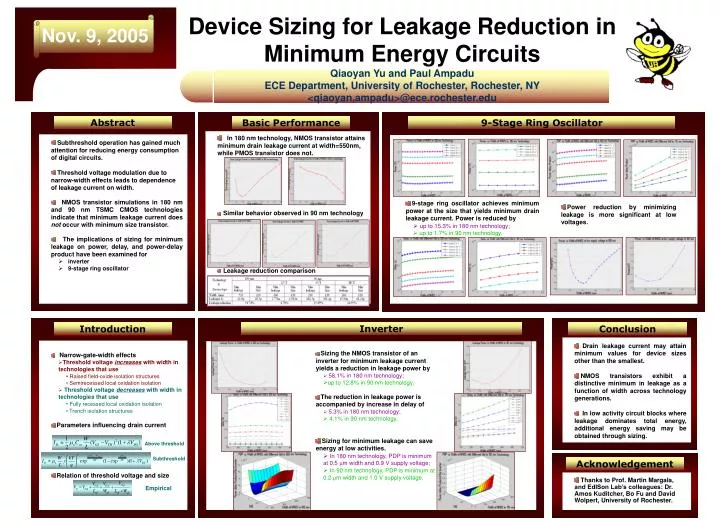
Device Sizing for Leakage Reduction in Minimum Energy Circuits Qiaoyan Yu and Paul Ampadu ECE Department, University of Rochester, Rochester, NY <qiaoyan,ampadu>@ece.rochester.edu. Abstract. Basic Performance. 9-Stage Ring Oscillator.

E N D
Device Sizing for Leakage Reduction in Minimum Energy Circuits Qiaoyan Yu and Paul Ampadu ECE Department, University of Rochester, Rochester, NY <qiaoyan,ampadu>@ece.rochester.edu Abstract Basic Performance 9-Stage Ring Oscillator • In 180 nm technology, NMOS transistor attains minimum drain leakage current at width=550nm, while PMOS transistor does not. • Similar behavior observed in 90 nm technology • Leakage reduction comparison • Subthreshold operation has gained much attention for reducing energy consumption of digital circuits. • Threshold voltage modulation due to narrow-width effects leads to dependence of leakage current on width. • NMOS transistor simulations in 180 nm and 90 nm TSMC CMOS technologies indicate that minimum leakage current does not occur with minimum size transistor. • The implications of sizing for minimum leakage on power, delay, and power-delay product have been examined for • inverter • 9-stage ring oscillator • 9-stage ring oscillator achieves minimum power at the size that yields minimum drain leakage current. Power is reduced by • up to 15.3% in 180 nm technology; • up to 1.7% in 90 nm technology. • Power reduction by minimizing leakage is more significant at low voltages. Inverter Introduction Conclusion • Drain leakage current may attain minimum values for device sizes other than the smallest. • NMOS transistors exhibit a distinctive minimum in leakage as a function of width across technology generations. • In low activity circuit blocks where leakage dominates total energy, additional energy saving may be obtained through sizing. • Narrow-gate-width effects • Threshold voltage increases with width in technologies that use • Raised field-oxide isolation structures • Semirecessed local oxidation isolation • Threshold voltage decreases with width in technologies that use • Fully recessed local oxidation isolation • Trench isolation structures • Parameters influencing drain current • Relation of threshold voltage and size • Sizing the NMOS transistor of an inverter for minimum leakage current yields a reduction in leakage power by • 58.1% in 180 nm technology; • up to 12.8% in 90 nm technology. • The reduction in leakage power is accompanied by increase in delay of • 5.3% in 180 nm technology; • 4.1% in 90 nm technology. • Sizing for minimum leakage can save energy at low activities. • In 180 nm technology,PDP is minimum at 0.5 mm width and 0.9 V supply voltage; • In 90 nm technology, PDP is minimum at 0.2 mm width and 1.0 V supply voltage. Above threshold Subthreshold Acknowledgement • Thanks to Prof. Martin Margala, and EdISon Lab’s colleagues: Dr. Amos Kuditcher, Bo Fu and David Wolpert, University of Rochester. Empirical