Download
1 / 43
2.04k likes | 5.24k Views
EXTRINSIC SEMICONDUCTOR In an extrinsic semiconducting material, the charge carriers originate from impurity atoms added to the original material is called impurity [or] extrinsic semiconductor.

E N D
EXTRINSIC SEMICONDUCTOR • In an extrinsic semiconducting material, the charge carriers originate from impurity atoms added to the original material is called impurity [or] extrinsic semiconductor. • This Semiconductor obtained by doping TRIVALENT and PENTAVALENT impurites in a TETRAVALENT semiconductor. The electrical conductivity of pure semiconductors may be changed even with the addition of few amount of impurities.
DOPING The method of adding impurities to a pure semiconductor is known as DOPING, and the impurity added is called the dopping agent(Ex-Ar,Sb,P,Ge and Al). The addition of impurity would increases the no. of free electrons and holes in a semiconductor and hence increases its conductivity. SORTS OF SEMICONDUCTOR according to ADDITION OFIMPURITIES n-type semiconductor p-type semiconductor
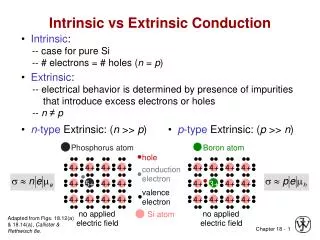
N – type semiconductor When pentavalent impurity is added to the intrinsic semiconductors, n type semi conductors are formed. At T = 0K n - type semiconductor
When small amounts of pentavalent impurity such as phosphorous are added during crystal formation, the impurity atoms lock into the crystal lattice[ see above Fig). • Consider a silicon crystal which is doped with a fifth column element such as P, As or Sb. • Four of the five electrons in the outermost orbital of the phosphorus atom take part in the tetrahedral bonding with the four silicon neighbours. • The fifth electron cannot take part in the discrete covalent bonding. It is loosely bound to the parent atom.
It is possible to calculate an orbit for the fifth electron assuming that it revolves around the positively charged phosphorus ion, in the same way as for the “1s” electron around the hydrogen nucleus. • The electron of the phosphorus atom is moving in the electric field of the silicon crystal and not in free space, as is the case in the hydrogen atom. • This brings in the dielectric constant of the crystal into the orbital calculations, and the radius of the electron orbit here turns out to be very large, about 80 Å, as against 0.5 Å for the hydrogen orbit. Such a large orbit evidently means that the fifth electron is almost free and is at an energy level close to the conduction band.
At OK, the electronic system is in its lowest energy state, all the valence electron will be in the valence band and all the phosphorous atoms will be un-ionised. • The energy levels of the donor atoms are very close to the conduction band. • In the energy level diagram, the energy level of the fifth electron is called donor level. The donor level is so close to the bottom of the conduction band. • Most of the donor level electrons are excited into the conduction band at room temperature and become majority charge carriers.
At T > 0K At T = 300K If the thermal energy is sufficiently high, in addition to the ionization of donor impurity atoms, breaking of covalent bonds may also occur thereby giving rise to generation of electron hole pair.
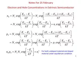
Fermi energy The Fermi energy for n – type semiconductor is given by At 0 K, Variation of Fermi level with temperature The Fermi energy is given by, Let
Variation of Fermi level with donor concentration with temperature • As T increases, Fermi level drops. Also for a given temperature the Fermi level shift upward as the concentration increases. • We can say that EF decreases slightly with increase in temperature. • As the temperature is increased, more and more donor atoms are ionized. For a particular temperature all the donor, atoms are ionized.
Further increase in temperature results in generation of electron-hole pairs due to the breaking of covalence bonds and the material tends to behave in intrinsic manner. The Fermi level gradually moves towards the intrinsic Fermi level Ei . P -Type Semiconductor When trivalent impurity is added to intrinsic semiconductor, P type semi conductors are formed. Al has three electrons in the outer orbital. While substituting for silicon in the crystal, it needs an extra- electron to complete the tetrahedral arrangement of bonds around it.
The extra electron can come only from one of the neighbouring silicon atoms, thereby creating a vacant electron site (hole) on the silicon. The aluminium atom with the extra electron becomes a negative charge and the hole with a positive charge can be considered to resolve around the aluminium atom, leading to the same orbital calculations as aboveT. p - type semiconductor At T = 0K
Since the trivalent impurity accepts an electron, the energy level of this impurity atom is called acceptor level. This acceptor level lies just above the valence bond. Even at relatively low temperatures, these acceptor atoms get ionized taking electrons from valence bond and thus giving to holes in the valence bond for conduction. Due to ionization of acceptor atoms, only holes and no electrons are created.
If the temperature is sufficiently high, in addition to the above process, electron-hole pairs are generated due to the breaking of covalent bonds. Thus holes are more in number than electrons and hence holes are majority carriers and electrons are minority carriers (a) At T > 0K (b) At T = 300K
Fermi Energy The Fermi energy for p – type semiconductor is given by At 0 K, At 0K, Fermi level is exactly at the middle of the acceptor level on the top of the valence band.
VARIATION OF FERMI LEVEL WITH TEMPERATURE = where Ny = 2 and therefore EF = From the above eqn, it is seen that EF increases slightly as the temperature increases. As the temperature increases, more and more acceptor atoms are ionised.
Na Na For a particular temperature all the acceptor atoms are ionized. Further increase in temperature results in generation of electron-hole pairdue to the breaking of covalent bonds and the material tend to behave in intrinsic manner. The Fermi level gradually moves towards the intrinsic Fermi level. Variation of Fermi level with acceptor concentration and temperature
Hall Effect When a piece of conductor (metal or semi conductor) carrying a current is placed in a transverse magnetic field, an electric field is producedinside the conductor in a direction normal to both the current and the magnetic field. This phenomenon is known as the Hall Effect and the generated voltage is called the Hall voltage. Hall effect
Consider a conventional current flow through the strip along OX and a magnetic field of induction B is applied along axis OY. • Case – I: If the Material is N-Type Semi Conductor (or) Metal • If the strip is made up of metal or N-type semiconductor, the charge carriers in the strip will be electrons. • As conventional current flows along OX, the electrons must be moving along XO. • If the velocity of the electrons is `v’ and charge of the electrons is `e’, the force on the electrons due to the magnetic field
F = Bev, which acts along OZ. • This causes the electrons to be deflected and the electrons accumulate at the face ABEF. • Face ABEF will become negative and the face OCDG becomes positive. • A potential difference is established across faces ABEF and OCDG, causing a field EH. Hall effect for n type semiconductor
This field gives rise to a force of `eEH’ on the electrons in the opposite direction. (i.e, in the negative Z direction) At equilibrium, eEH = Be(or) EH = B If J is the current density, then, J = ne where `n’ is the concentration of current carriers. v = Substitute the value of `’ in eqn EH =
The Hall Effect is described by means of the Hall coefficient `RH’ in terms of current density `J’ by the relation, EH = RHBJ (or) RH = EH/ BJ All the three quantities EH, J and B are measurable, the Hall coefficient RH and hence the carrier density `n’ can be found out.
Case – (ii) If the material is a P-type semi conductor • If the strip is a P-type semiconductor, the charge carriers in the strip will be holes. • The holes will constitute current in the direction of conventional current. • Holes move along the direction of the conventional current itself along ox Hall effect for p type semiconductor
If `e’ is the charge of the hole, the force experienced by the holes due to magnetic field is, F = Be , which acts along OZ. This causes the holes to accumulate on the face ABEF – making it positive, and leaving the face OCDG as negative. P-type semiconductor,RH = 1/pe , where p = the density of holes.
Determination of Hall coefficient The Hall coefficient is determined by measuring the Hall voltage that generates the Hall field. If `w’ is the width of the sample across which the Hall voltage is measured, then EH = VH/ w We know that, RH = EH/ BJ Substituting the value of EH in the above eqn RH = VH/ wBJ (or) VH = RHwBJ
If the thickness of the sample is `t’, the its cross sectional area A = wt, and the current density, J= Substitute the value of `J ’ VH = = (or) RH = VH will be opposite in sign for P and N type semiconductors.
A rectangular slab of the given material having thickness `t’ and width `w’ is taken. A current of `I’ amperes is passed through this sample by connecting it to a battery, `Ba’. The sample is placed between two pole pieces of an electromagnet such that the field `B’ is perpendicular toI
The hall voltage `VH’ is then measured by placing two probes at the two side faces of the slab. If the magnetic flux density is `B’ and `VH’ is the hall voltage, then the Hall coefficient, Experimental setup for the measurement of Hall voltage
RH = VHt / IB (m3/coulomb) For n-type material, n = nee (or) For p-type material, p = p e h(or)
Applications of Hall effect (1) Determination of N-type of semiconductor For a N-type semiconductor, the Hall coefficient is negative whereas for a P-type semiconductor, it is positive. Thus from the direction of the Hall voltage developed, one can find out the type of semiconductor. (2) Calculation of carrier concentration Once Hall coefficient RH is measured, the carrier concentration can be obtained,
Determination of mobility • We know that, conductivity, n = n ee (or) Also, P = p eh (or) Thus by measuring `’ and RH, ’ can be calculated. (4) Measurement of magnetic flux density. Using a semiconductor sample of known `RH’, the magnetic flux density can be deduced from, RH=
DILUTE MAGNETIC SEMICONDUCTORS • Introduction • Integrated circuits and high-frequency devices made of semiconductors, used for information processing and communications, have had great success using the charge of electrons in semiconductors.
Mass storage of information–indispensable for information technology–is carried out by magnetic recording (hard disks, magnetic tapes, magneto optical disks) using spin of electrons in ferromagnetic materials. • Dilute or diluted magnetic semiconductors (DMS) also referred to as semi magnetic semiconductors, are alloys whose lattices are made up in part of substitutional magnetic atoms. • DMS= Semiconductors with dilute concentration of magnetic dopants.
The most important feature of these materials is carrier mediated magnetism which can be easily controlled with voltage. The advantage is that, unlike the conventional magnets, DMS are compatible with semiconductors and can be used as efficient sources for spin injection. Three types of semiconductors: (A) a magnetic semiconductor(e.g. some spinels), in which a periodic array of magnetic element is present, (B) a dilute magnetic semiconductor(e.g. (GaMn)As,(InMn)P, ZnCoO etc), an alloy between nonmagnetic semiconductor and magnetic element and (C) a non-magnetic semiconductor(e.g. GaAs, InP, Cu2O, NiO etc), which contains no magnetic ions.
Materials The most common SMSC are II-VI compounds (like CdTe, ZnSe, CdSe, CdS, etc.), with transition metal ions (e.g. Mn, Fe or Co) substituting their original cations. There are also materials based on IV-VI (e.g. PbTe, SnTe) and recently III-V (e.g. GaAs, InSb) crystals. The wide variety of both host crystals and magnetic atoms provides materials which range from wide gap to zero gap semiconductors, and which reveal many different types of magnetic interaction. Formation of DMS
Several of the properties of these materials may be tuned by changing the concentration of the magnetic ions. The most relevant feature of DMS, is the coexistence and interaction of two different electronic sub systems: delocalized conduction (s-type) and valence (p-type) band electrons and localized (d or f-type) electrons of magnetic ions. In particular the spd exchange interaction leads to strong band splitting, which result in giant magneto optical effects .
The most studied III-V DMS system is GaxMn1-xAs with xup to 0.07. The solubility limit of magnetic elements in III-V semiconductors is very low, but in order to have ferromagnetism in DMS, a sizable amount of magnetic ions are needed. This can only be accomplished by means of nonequilibrium crystal growth techniques, such as low temperature molecular beam epitaxy (MBE). The upper concentration limit of magnetic ions is around 10 %.
The highest conclusively reported Tc of DMS is around 110 K for 5 % doped GaAs. It is of great technological importance to find DMS systems with Tc above room temperature, before one attempts to make a DMS based device. Applications Diluted magnetic semiconductors (DMS) are expected to play an role in interdisciplinary materials science and future electronics because charge and spin degrees of freedom accommodated into a single material exhibits interesting magnetic, magneto-optical, magnetoelectronic and other properties.
It is expected that magnetoelectronic important chips will be used in quantum computers. An inherent advantage of magnetoelectronics over electronics is the fact that magnet tend to stay magnetized for long. Hence this arises interest in industries to replace the semiconductor-based components of computer with magnetic ones, starting from RAM. These DMS materials are very attractive for integration of photonic (light-emitting diodes), electronic (field effect transistors), and magnetic (memory) devices on a single substrate.
Some important application areas of DMS are listed below. • Photonics plus spintronics (Spin+electronics = Spintronics) • Improved spin transistor • Transistors spin toward quantum computing • Magnetic spins to store quantum information • Microscope to view magnetism at atomic level
Ballistic magneto resistance • Missile guidance • Fast accurate position and motion sensing of mechanical components in precision aengineering and in robotics • In automotive sensors
Importance of DMS based devices • Information is stored (written) into spins as a particular spin orientation (up or down) • The spins, being attached to mobile electrons, carry the information along a conductor • The information can be stored or is read at a terminal. • Spintronics devices are attractive for memory storage and magnetic sensors applications
Spin-based electronics promises a radical alternative to charge-based electronics, namely the possibility of logic operations with much lower power consumption than equivalent charge-based logic operations