Download
1 / 10
110 likes | 383 Views
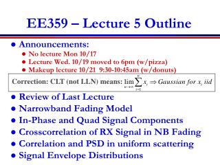
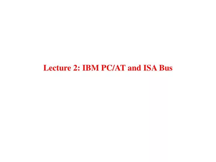
Lecture 2: IBM PC/AT and ISA Bus. 80386- based PC/AT-Compatible System. DRAM. 82345 Data Buffer. 386 DX+82340 chip set. 386 DX. SYSTEM BUS. LOCAL BUS. 82346 System Controller. 82341 Peripheral Combo. 387 DX. 82344 ISA Controller. 82385 DX Cache Controller. Cache. BIOS.

E N D
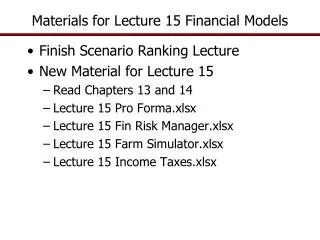
80386-based PC/AT-Compatible System DRAM 82345 Data Buffer 386DX+82340 chip set 386DX SYSTEM BUS LOCAL BUS 82346 System Controller 82341 Peripheral Combo 387 DX 82344 ISA Controller 82385DX Cache Controller Cache BIOS Industry Standard Architecture(ISA) Bus
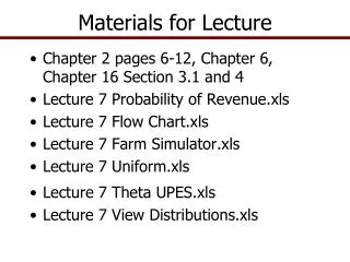
Pentium Processor/82430 PCIset ISA Host Bus Pentium Processor CNTL ADDR DATA Latch 82434 PCMC 82433 LBX DRAM SRAM PCI BUS CNTL ADDR/DATA 82378 SIO Grahics PCI devices ISA BUS
Block Diagram of the System Board • All signal lines are TTL compatible. Fan-out are two low power Shottkey(LS) TTLs. • SA0 through SA19: System Address Bus:(I/O) • to address memory and I/O devices; 16MB of memory with LA17 through LA23 • input when CPUHLDA is high and MASTER* is low; output at all other times • SA bus driven by CPU when CPUHLDA is low; SA bus driven by 8237 DMA controller when CPUHLDA is high • latched with an internally generated ALE signal External Master data CPU addr ISA Bus Memory addr data MEM DMA I/O
LA17 through LA23 (Latchable Address Bus); I/O • the same as SA19-SA0 • MEMR* (Memory Read, active low); I/O • Input when CPUHLDA is high and MASTER* is low • it is driven from the 288 bus controller when CPUHLDA is low and MASTER* is high • it is driven by the 8237 DMA controller when CPUHLDA is high and MASTER* is high • requires an external 10K pull-up registor • MEMW*(Memory Write, active low): I/O • Input/output determination: the same as MEMR* • requires an external 10K pull-up registor • SMEMR*(Memory Read): I/O • Input/Output determination: the same as MEMR* • active on memory read cycles to addresses below 1 MB. • requires an external 10KW pull-up registor • SMEMW*(Memory Write):I/O • Input/Output determination: the same as MEMR* • active on memory read cycles to addresses below 1 MB. • requires an external 10K pull-up registor • SBHE*(System Byte High Enable) : I/O • controlled the same way as the SA bus
REFRESH*(Refresh signal); I/O • SYSCLK(System CLock) : O • this output is half the frequency of the BUSCLK input • BALE, IOR*, IOW*, MEMR*, MEMW* are synchronized to SYSCLK • OSC(Oscillator): I-TTL • the buffered inout of the external 14.318 MHz oscillator. • RSTDRV(Reset Drive): O • BALE(Buffered Address Latch Enable): O • A pulse which is generated at the beginning of any bus cycle initiated from the CPU. • AEN (Address Enable): O • goes high anytime the inputs CPUHLDA and MASTER* are both high • DMA controller has control when this signal is active • T/C (Terminal Count): O • indicates that one of the DMA channels terminal count has been reached • DACK7*- DACK5*, DACK3*- DACK0* (DMA Acknowledge): O • DRQ7-DRQ5, DRQ3-DRQ0 (DMA Request) : I • DRQ0-DRQ3 : from 8-bit I/O adapters to/from system memory • DRQ5-DRQ7: from 16-bit I/O to/from system memory • DRQ4 is not available externally as it is used to cascade the two DMA controllers together.
IRQ15-IRQ9, IRQ7-IRQ3, IRQ1 (Interrupt Request) : I • inputs for the 8259 megacells • IRQ0, IRQ2, IRQ8 ; not available as external inputs • MASTER* (Master) : I • used by an external device to disable the internal DMA controllers and get access to the system bus • when asserted it indicates that an external bus master has control of the bus. • MEMCS16* (Memory Chip Select 16-bit) : I • used to determine when a 16-bit to 8-bit conversion is needed for CPU addresses • A 16 to 8 conversion is done anytime the System Controller requests a 16-bit memory cycle and MASTER* is sampled high. • IOCS16* (I/O Chip Select 16-bit) : I • functions the same way as MEMCS16* signals • IOCHK* (I/O Channel Check): I • used to indicate that an error has taken place on the I/O bus • IOCHRDY (I/O Channel Ready) : I • pulled low in order to extend the read or write cycles of any bus access when required • the default number of wait states for cycles initiated by the CPU; • four wait states for 8-bit peripherals • one wait state for 16-bit peripherals • three wait states for ROM cycles • One wait state is inserted as the default for all DMA cycles
WS0* (Wait State 0) : I • pulled low by a peripheral on the bus to terminate a CPU controlled bus cycle earlier than the default values