Download
1 / 15
150 likes | 156 Views
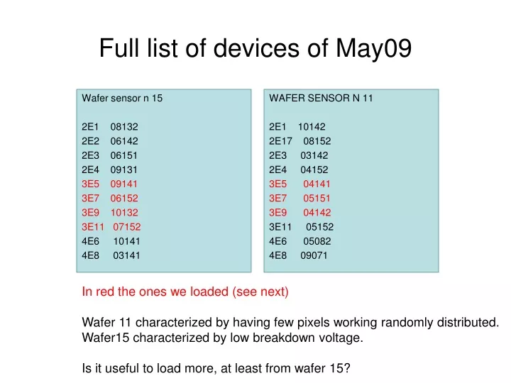
Full list of devices of May09. Wafer sensor n 15 2E1 08132 2E2 06142 2E3 06151 2E4 09131 3E5 09141 3E7 06152 3E9 10132 3E11 07152 4E6 10141 4E8 03141. WAFER SENSOR N 11 2E1 10142 2E17 08152 2E3 03142 2E4 04152 3E5 04141

E N D
Full list of devices of May09 Wafer sensor n 15 2E1 08132 2E2 06142 2E3 06151 2E4 09131 3E5 09141 3E7 06152 3E9 10132 3E11 07152 4E6 10141 4E8 03141 • WAFER SENSOR N 11 • 2E1 10142 • 2E17 08152 • 2E3 03142 • 2E4 04152 • 3E5 04141 • 3E7 05151 • 3E9 04142 • 3E11 05152 • 4E6 05082 • 4E8 09071 In red the ones we loaded (see next) Wafer 11 characterized by having few pixels working randomly distributed. Wafer15 characterized by low breakdown voltage. Is it useful to load more, at least from wafer 15?
Some more tests on the three devices of wafer 15 that we still have in Genova: • Repeat IV scan • Noise vs HV • Monleak scan • Xtalk (done but not understood yet) Noise, monleak and Xtalk only for two devices as one as the FE not working. IV curves for three devices of wafer 15. Vbd is ~10V.
Wafer15: 3e11_07152 • Noise vs HV • Monleak
20 V The noise becomes higher, especially when two neighbouring pixels are injected at the same time. Increasing the voltage, the noisy area increases. 12 V At 10V the leakage voltage starts raising, few pixels starts becoming very noisy 10 V 8 V
Monleak@8V 2D Noise map
Monleak@10V Three pixels show an higher leakage current and their noise starts increasing (also for few neighbours)
Monleak@16V The areas of noise increase around the noisy “pixel seeds’
Wafer15: 3E9_10132 • Noise vs HV • Monleak
Noise map vs HV 18 V 12 V Two areas are visible where the noise increases 10 V 8 V Many pixels are noisy already at low voltages
Outlook • Wafer 15 have a low breakdown voltage. This seems correlated to few pixels that start drawing more current. It does not look as a coherent effect or due to cut problem. • Debug the FE not working • Load more? Is it useful to get more evidence? • Understand better the Xtalk results (not shown)