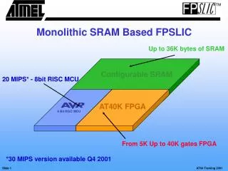
Download

1 / 23
260 likes | 448 Views
McKenneman, Inc. SRAM Proposal. Design Team: Jay Hoffman Tory Kennedy Sholanda McCullough. Outline. Introduction Design Approach Schematics Block Design Top-level Design Layout Bitcell Layout Peripheral and Block Layout Simulation SNM simulations of bitcell Block simulations

E N D
McKenneman, Inc.SRAM Proposal Design Team: Jay Hoffman Tory Kennedy Sholanda McCullough
Outline • Introduction • Design Approach • Schematics • Block Design • Top-level Design • Layout • Bitcell Layout • Peripheral and Block Layout • Simulation • SNM simulations of bitcell • Block simulations • Problems Encountered • Metric Analysis • Conclusion
Design Approach • Low Power SRAM running at Vdd = 2.5V • Power gating on idle blocks • 1Mb of memory • Made of 32 blocks of 128x256 bits • 32bit words addressed with 15bits • Voltage sense amp to reduce precharge power • Minimizing bitcell layout to reduce overall size
Block Features • 7:128 row address decoder raises the WL • 3:8 decoder selects the 32 columns to when writing to the memory • Each bitline has a sense amp to reduce the time each WL is enabled and reduce the amount of precharging • A chain of 32 8:1 muxes after the sense amps selects the word on a read operation • A register latches the block output and is wired to a tri-state buffer, allowing all blocks to share one SRAM output
Top-Level Features • 5bits of address choose the block • Read, Write, and input addresses are held by registers • Applying the philosophy of designing for controllability, precharge and sense amp enable are pinned out • Designing for observability, a sense amp’s output is pinned out for timing verification
Bitcell Features • Dimensions: 19.8 microns by 8.4 microns • Area: 166.32 microns^2 • Area is saved in the array by overlapping mirrored bitcells every other row to share ground and vdd connections
Sense Amp Features • 21 microns wide • Designed to be same width as bitcell so it can be easily wired to the array
4:16 Features • 5 2:4 decoders combined • 8 of these make up 7:128 decoder • 100 microns long to connect with buffers to the memory array
Block Statistics • Dimensions estimated to be 5478 microns by 1415 microns • Approximate Area: 7,751,370 microns^2 • Includes memory array, 7:128 decoder, WL buffers, precharge, sense amps, output buffers • Extra room estimated for registers, tri-state buffers, smaller logic
SNM Bitcell Simulations • Length of the side of largest square inside curves • Best Case: SF • Read: .651 • Hold: .940 • Worst Case: FS • Read: .480 • Hold: .792 Hold case for a SF bitcell
Block Sim Notes R/W/R • First line shows CLK and Output of Tri-state buffer after a read • Second line show BL(blue) and BLB(red) • Third line shows Sense Amps firing and their output • Fourth line shows WL enabled inside of precharge • Fifth line shows read/write signals
6 Access for block • Writes a one into a block and reads it 5 times for total average power of 31 mW • Total time for D-Q is 15.5 ns • The output is latched on rising clock edge, with 2.5ns to propagate through register and tri-state buffer
Problems Encountered • Clock distribution • Measuring enough clock delays to fire sense amps at the correct time • Delaying and buffering the precharge • Slow simulation times • Wiring and reducing layouts
Metric Analysis • Average power of 1 write and 5 reads: .031W • Largest delay: 13ns • Total Area: 32*(7,751,370 microns^2) = 248,043,840 microns^2 • Metric= (Watts^2)*(delay in ns)*(area in um^2) • McKenneman’s Score=3.099E6
Conclusion • McKenneman, Inc. has developed an efficient and power saving SRAM design • Special Features • Low voltage operation • Design for controllability and observability • Block enable signal power gates idle blocks